 | –≠–ª–µ–∫—Ç—Ä–æ–Ω–Ω—ã–π –∫–æ–º–ø–æ–Ω–µ–Ω—Ç: CXP973064 | –°–∫–∞—á–∞—Ç—å:  PDF PDF  ZIP ZIP |
CMOS 16-bit Single Chip Microcomputer
Description
The CXP972032/973032/973064 is a CMOS 16-bit
microcomputer integrating on a single chip an A/D
converter, serial interface, I
2
C bus interface, timer,
PWM output circuit, programmable pattern
generator, remote control receive circuit, parallel
interface, as well as basic configurations like a 16-bit
CPU, ROM, RAM, and I/O port.
This LSI also provides the sleep/stop functions that
enable lower power consumption.
Features
∑ An efficient instruction set as a controller
-- Direct addressing, numerous abbreviated forms,
multiplication and division instructions
∑ Instruction sets for C language and RTOS
-- Highly quadratic instruction system,
general-purpose register of 16-bit
◊
8-pin
◊
16-bank
configuration
∑ Minimum instruction cycle
50ns at 40MHz operation (2.7 to 3.6V)
∑ Incorporated ROM capacity
128K bytes (CXP972032/973032)
256K bytes (CXP973064)
∑ Incorporated RAM capacity
7.5K bytes (CXP972032)
11.5K bytes (CXP973032/973064)
∑ Peripheral functions
-- A/D converter
8-bit 12-analog input, successive approximation system,
3-stage FIFO (Conversion time: 1.55µs at 40MHz)
-- Serial interface
Asynchronous serial interface (UART)
128-byte buffer RAM, 3 channels
-- I
2
C bus interface
64-byte buffer RAM
(supports master/slave and automatic transfer mode)
-- Timers
8-bit timer/counter, 2 channels (with timing output)
16-bit capture timer/counter (with timing output)
16-bit timer, 4 channels, watchdog timer
-- PWM output circuit
14-bit PWM, 4 channels
(2 channels of binary output switch function by PPG)
-- Programmable pattern generator
16-bit output, 64-byte buffer RAM, 1 channel
-- Remote control receive circuit
8-bit pulse measurement counter, 10-stage FIFO
-- Parallel interface
External register interface (8-bit parallel bus), 4-chip select
∑ Interruption
33 factors, 33 vectors, multi-interruption and priority selection possible
∑ Standby mode
Sleep/stop
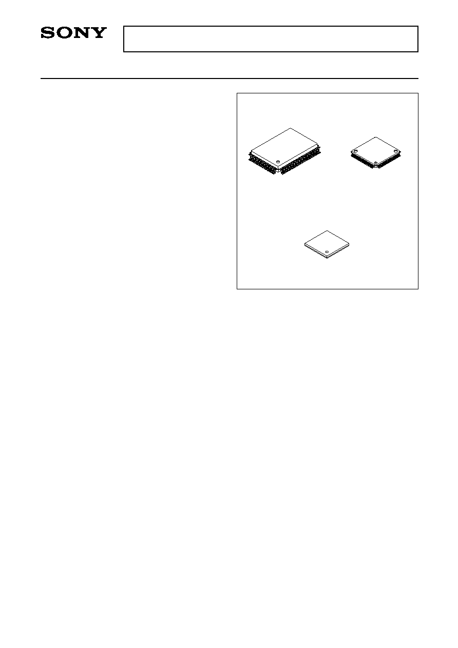
∑ Package
100-pin plastic QFP (CXP972032/973032/973064)
100-pin plastic LQFP (CXP972032/973032/973064)
104-pin plastic LFLGA (CXP973064)
∑ Piggy/evaluation chip
CXP971000
∑ FLASH EEPROM incorporated version CXP973F064
Structure
Silicon gate CMOS IC
≠ 1 ≠
E99930A14-PS
Sony reserves the right to change products and specifications without prior notice. This information does not convey any license by
any implication or otherwise under any patents or other right. Application circuits shown, if any, are typical examples illustrating the
operation of the devices. Sony cannot assume responsibility for any problems arising out of the use of these circuits.
CXP972032/973032/973064
100 pin QFP (Plastic)
100 pin LQFP (Plastic)
104 pin LFLGA (Plastic)
Perchase of Sony's I
2
C components conveys a licence under the Philips I
2
C Patent Rights to use these components
in an I
2
C system, provided that the system conforms to the I
2
C Standard Specifications as defined by Philips.
≠ 2 ≠
CXP972032/973032/973064
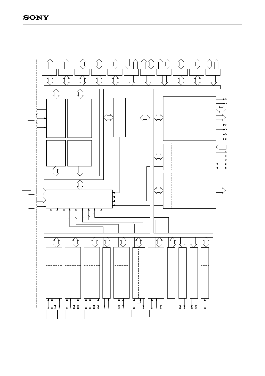
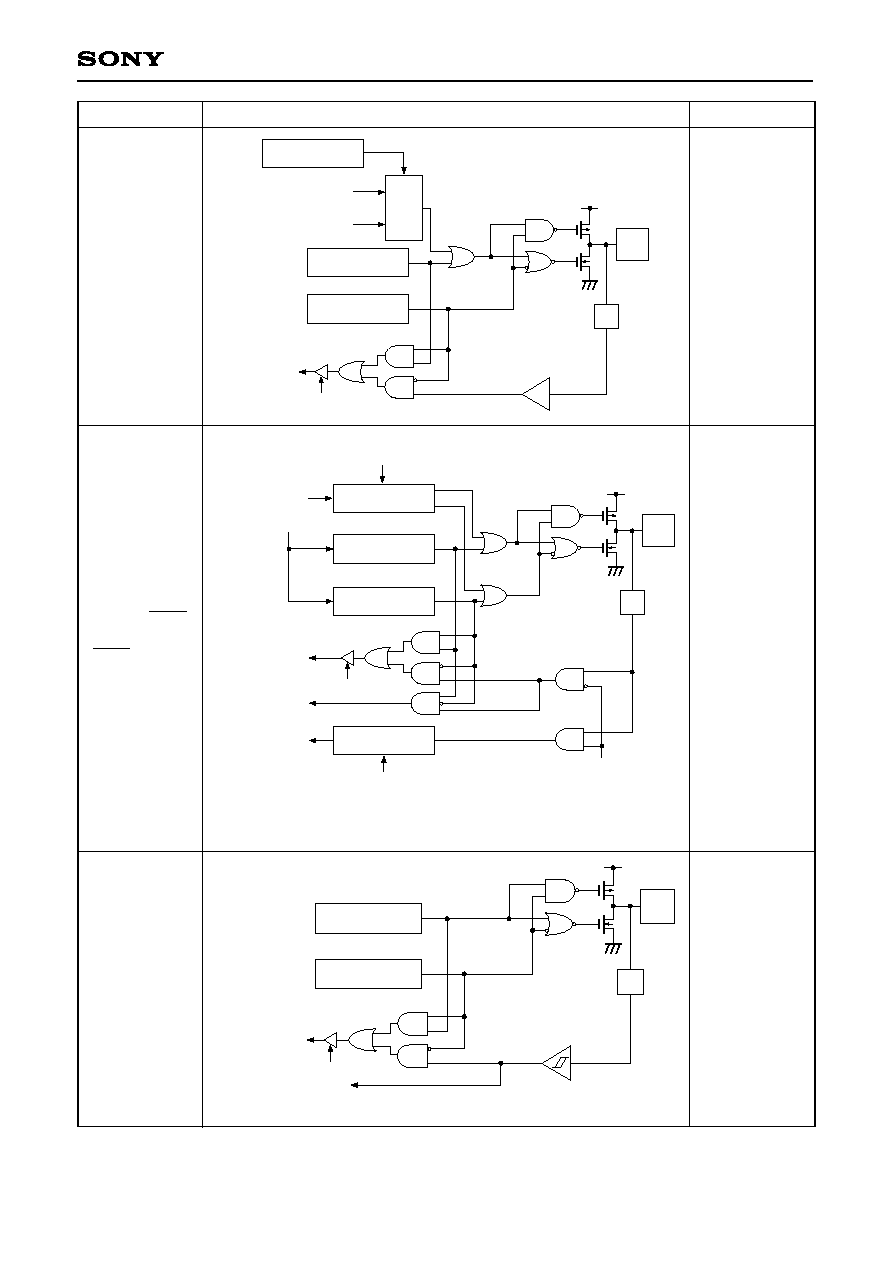
Block Diagram
P
A
0 to P
A
7
PB0 to PB7
PC0 to PC7
PD0 to PD7
PE0 to PE7
PF0 to PF5
PF6, PF7
PH0, PH1,
PH6, PH7
PI0 to PI7
PJ0 to PJ7
SCS0
SO0
SI0
SCK0
SI1
SCS1
SCK1
SO1
SCS2
SO2
SI2
SCK2
T1
PWM0
EC0
RMC
PORT
A
16-BIT
CAPTURE
TIMER/COUNTER (CH2)
BUFFER
RAM
I
2
C BUS
INTERF
A
CE
UNIT
BUFFER
RAM
SERIAL
INTERF
A
CE
UNIT
(CH2)
BUFFER
RAM
SERIAL
INTERF
A
CE
UNIT
(CH1)
BUFFER
RAM
SERIAL
INTERF
A
CE
UNIT
(CH0)
8
8
20
PORT
B
8
PORT
C
8
PORT
D
8
PG4 to PG7
4
PH2 to PH5
4
PORT
E
8
PORT
F
6
2
PG0 to PG3
4
4
PORT
G
PK0 to PK4
5
PK5 to PK6
2
PORT
K
PORT
H
PORT
I
PORT
J
8
8
SPC970
CPU CORE
CLOCK GENERA
T
O
R/
SYSTEM CONTROLLER
ROM
128K/256K
BYTES
RAM
7.5K/1
1.5K
BYTES
PWM1
PWM2
PWM3
T2
PRESCALER/
TIME-BASE TIMER
EC2
CINT
SCL
SDA
TxD
RxD
INT0
to INT7
KS0
to KS19
NMI
RST
EXTAL
XTAL
V
DD
V
SS
16
A/D
CONVER
TER
12
8
REMOCON
FIFO
2CH 14-BIT
PWM (PPG)
2CH 14-BIT
PWM
4CH 16-BIT
TIMER
UAR
T
INTERRUPT CONTROLLER
AN0
to AN11
PPO00
to PPO15
16
D0 to D7
A0 to A15
ADTEN
ADTRG
XCS3
XCS2
XCS1
XCS0
XRD
XWR
AV
SS
AV
REF
AV
DD
8-BIT
TIMER/COUNTER
(CH0)
8-BIT
TIMER
(CH1)
2
4
2
3
2
PROGRAMABLE
P
A
TTEERN
GENERA
T
O
R
EXT
.
REGISTERS
INTERF
ACE
BUFFER RAM
FIFO
T
O
KEI PRESCALER
≠ 3 ≠
CXP972032/973032/973064
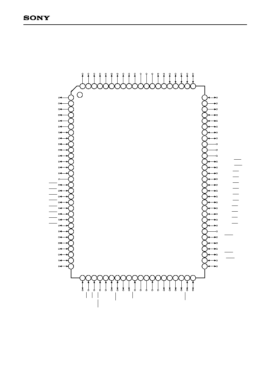
Pin Assignment 1 (Top View) 100-pin QFP package
31 32 33 34 35 36 37 38 39 40 41 42 43 44 45 46 47 48 49 50
57
58
59
60
61
62
63
64
65
66
67
68
69
70
71
72
73
74
75
76
77
78
79
80
81
82
83
84
85
86
87
88
89
90
91
92
93
94
95
96
97
98
99
1
2
3
4
5
6
7
8
9
10
11
12
13
14
15
16
17
18
19
20
21
22
23
24
PE7/INT7/CINT
PF0/EC0
PF1/EC2
PF2/SCS1/NMI
PF3/SI1
PF4/SO1
PF5/SCK1
PF6/T1
PF7/T2
RST
V
SS
XT
AL
EXT
AL
V
DD
PG0/PWM0
PG1/PWM1
PG2/PWM2
PG3/PWM3
PG4/SCS0
PG5/SI0
PH0/SDA
PK6
PK5
PK4/ADTRG
PK3/ADTEN
PK2
PK1
PK0
AV
DD
AV
REF
AV
SS
PJ7/AN11/KS11
PJ6/AN10/KS10
PJ5/AN9/KS9
PJ4/AN8/KS8
PJ3/AN7/KS7
PJ2/AN6/KS6
PJ1/AN5/KS5
PJ0/AN4/KS4
PI7/AN3/KS3
PI6/AN2/KS2
PI5/AN1/KS1
PI4/AN0/KS0
Vss
PI3/SCK2
51
52
53
54
55
56
PI2/SO2
PI1/SI2
PI0/SCS2
PG7/SCK0
PG6/SO0
PB2/PPO02/A10
PB3/PPO03/A11
PB4/PPO04/A12
PB5/PPO05/A13
PB6/PPO06/A14
PB7/PPO07/A15
PC0/PPO08
PC1/PPO09
PC2/PPO10
PC3/PPO11
PC4/PPO12/XCS3
PC5/PPO13/XCS2
PC6/PPO14/XCS1
PC7/PPO15/XCS0
V
SS
PD0/D0/KS12
PD1/D1/KS13
PD2/D2/KS14
PD3/D3/KS15
PD4/D4/KS16
PD5/D5/KS17
PD6/D6/KS18
PD7/D7/KS19
PE0/INT0
25
26
27
28
29
PE1/INT1
PE2/INT2
PE3/INT3
PE4/INT4
PE5/INT5
30
PE6/INT6
PB1/PPO01/A9
PB0/PPO00/A8
P
A7/A7
P
A6/A6
P
A5/A5
P
A4/A4
P
A3/A3
P
A2/A2
P
A1/A1
P
A0/A0
V
SS
V
DD
NC
PH7/XRD
PH6/XWR
PH5
PH4/RMC
PH3/TxD
PH2/RxD
PH1/SCL
100
Note) 1. NC (Pin 88) must be left open. However, use this pin for FLASH EEPROM
incorporated version.
2. Vss and AVss (Pins 15, 41, 57, 70 and 90) must be connected to GND.
3. V
DD
and AV
DD
(Pins 44, 72 and 89) must be connected to V
DD
.
≠ 4 ≠
CXP972032/973032/973064
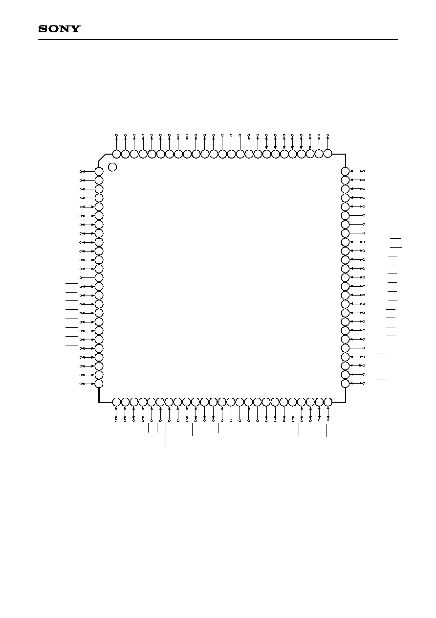
Pin Assignment 2 (Top View) 100-pin LQFP package
31 32 33 34 35 36 37 38 39 40 41 42 43 44 45 46 47 48 49 50
57
58
59
60
61
62
63
64
65
66
67
68
69
70
71
72
73
74
75
76
77
78
79
80
81
82
83
84
85
86
87
88
89
90
91
92
93
94
95
96
97
98
99
1
2
3
4
5
6
7
8
9
10
11
12
13
14
15
16
17
18
19
20
21
22
23
24
PE7/INT7/CINT
PF0/EC0
PF1/EC2
PF2/SCS1/NMI
PF3/SI1
PF4/SO1
PF5/SCK1
PF6/T1
PF7/T2
RST
V
SS
XT
AL
EXT
AL
V
DD
PG0/PWM0
PG1/PWM1
PG2/PWM2
PG3/PWM3
PG4/SCS0
PG5/SI0
PH0/SDA
PK6
PK5
PK4/ADTRG
PK3/ADTEN
PK2
PK1
PK0
AV
DD
AV
REF
AV
SS
PJ7/AN11/KS11
PJ6/AN10/KS10
PJ5/AN9/KS9
PJ4/AN8/KS8
PJ3/AN7/KS7
PJ2/AN6/KS6
PJ1/AN5/KS5
PJ0/AN4/KS4
PI7/AN3/KS3
PI6/AN2/KS2
PI5/AN1/KS1
PI4/AN0/KS0
Vss
PI3/SCK2
51
52
53
54
55
56
PI2/SO2
PI1/SI2
PI0/SCS2
PB4/PPO04/A12
PB5/PPO05/A13
PB6/PPO06/A14
PB7/PPO07/A15
PC0/PPO08
PC1/PPO09
PC2/PPO10
PC3/PPO11
PC4/PPO12/XCS3
PC5/PPO13/XCS2
PC6/PPO14/XCS1
PC7/PPO15/XCS0
V
SS
PD0/D0/KS12
PD1/D1/KS13
PD2/D2/KS14
PD3/D3/KS15
PD4/D4/KS16
PD5/D5/KS17
PD6/D6/KS18
PD7/D7/KS19
PE0/INT0
25
26 27 28 29
PE1/INT1
PE2/INT2
PE3/INT3
30
PE4/INT4
PE5/INT5
PE6/INT6
PB1/PPO01/A9
PB2/PPO02/A10
PB3/PPO03/A1
1
PB0/PPO00/A8
P
A
7/A7
P
A
6/A6
P
A
5/A5
P
A
4/A4
P
A
3/A3
P
A
2/A2
P
A
1/A1
P
A
0/A0
V
SS
V
DD
NC
PH7/XRD
PH6/XWR
PH5
PH4/RMC
PH3/TxD
PH2/RxD
PH1/SCL
100
PG7/SCK0
PG6/SO0
Note) 1. NC (Pin 86) must be left open. However, use this pin for FLASH EEPROM
incorporated version.
2. Vss and AVss (Pins 13, 39, 55, 68 and 88) must be connected to GND.
3. V
DD
and AV
DD
(Pins 42, 70 and 87) must be connected to V
DD
.
≠ 5 ≠
CXP972032/973032/973064
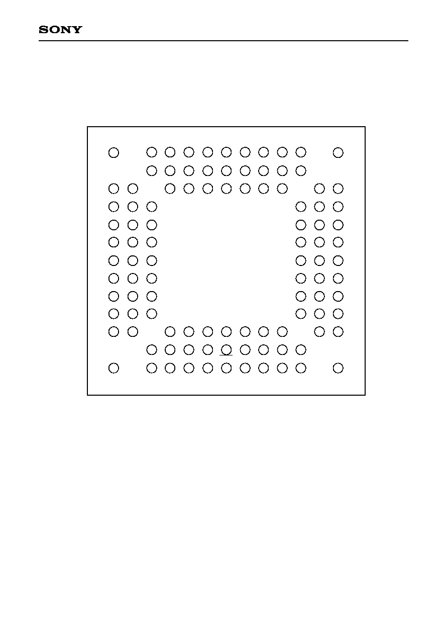
Pin Assignment 3 (Top View) 104-pin LFLGA package
3
100
2
1
5
4
6
7
8
9
10
13
12
11
15
16
14
17
18
19
20
21
22
24
23
28
25
27
26
29
30
32
31
33
35
34
38
37
36
39
40
41
42
43
46
44
45
47
49
48
53
50
52
51
55
54
56
57
58
60
59
61
62
63
64
65
66
67
68
71
69
70
72
74
73
78
75
77
76
80
79
81
82
83
85
84
88
87
86
90
91
89
92
93
94
95
96
97
99
98
1
2
3
4
5
6
7
8
9
10
11
12
13
PB0
PA6
PA3
PA1
V
DD
PH6
PH4
PH2
PK6
A
PB2
PA7
PA4
PA2
V
SS
PH7
PH3
PK5
PK4
B
PB5
PB3
PB1
PA5
PA0
NC
PH5
PH1
PH0
PK3
PK1
C
PC0
PB4
PB6
PK2 AV
DD
AV
REF
D
PC2
PC1
PB7
PK0 AV
SS
PJ7
E
PC5
PC4
PC3
PJ6
PJ5
PJ4
F
PC7
V
SS
PC6
PJ3
PJ1
PJ2
G
PD1
PD2
PD0
PI6
PJ0
PI7
H
PD3
PD4
PD5
PI3
PI4
PI5
J
PD6
PD7
PE1
PI2
PI0
V
SS
K
PE0
PE2
PE6
PF0
PF3
PF6 EXTAL PG3
PG5
PG7
PI1
L
PE3
PE4
PF2
PF5
RST XTAL
PG0
PG2
PG6
M
PE5
PE7
PF1
PF4
PF7
V
SS
V
DD
PG1
PG4
N
Note) 1. NC (Pin C7) must be left open. However, use this pin for FLASH EEPROM
incorporated version.
2. Vss and AVss (Pins B7, E12, G2, K13 and N8) must be connected to GND.
3. V
DD
and AV
DD
(Pins A7, D12 and N9) must be connected to V
DD
.
≠ 6 ≠
CXP972032/973032/973064
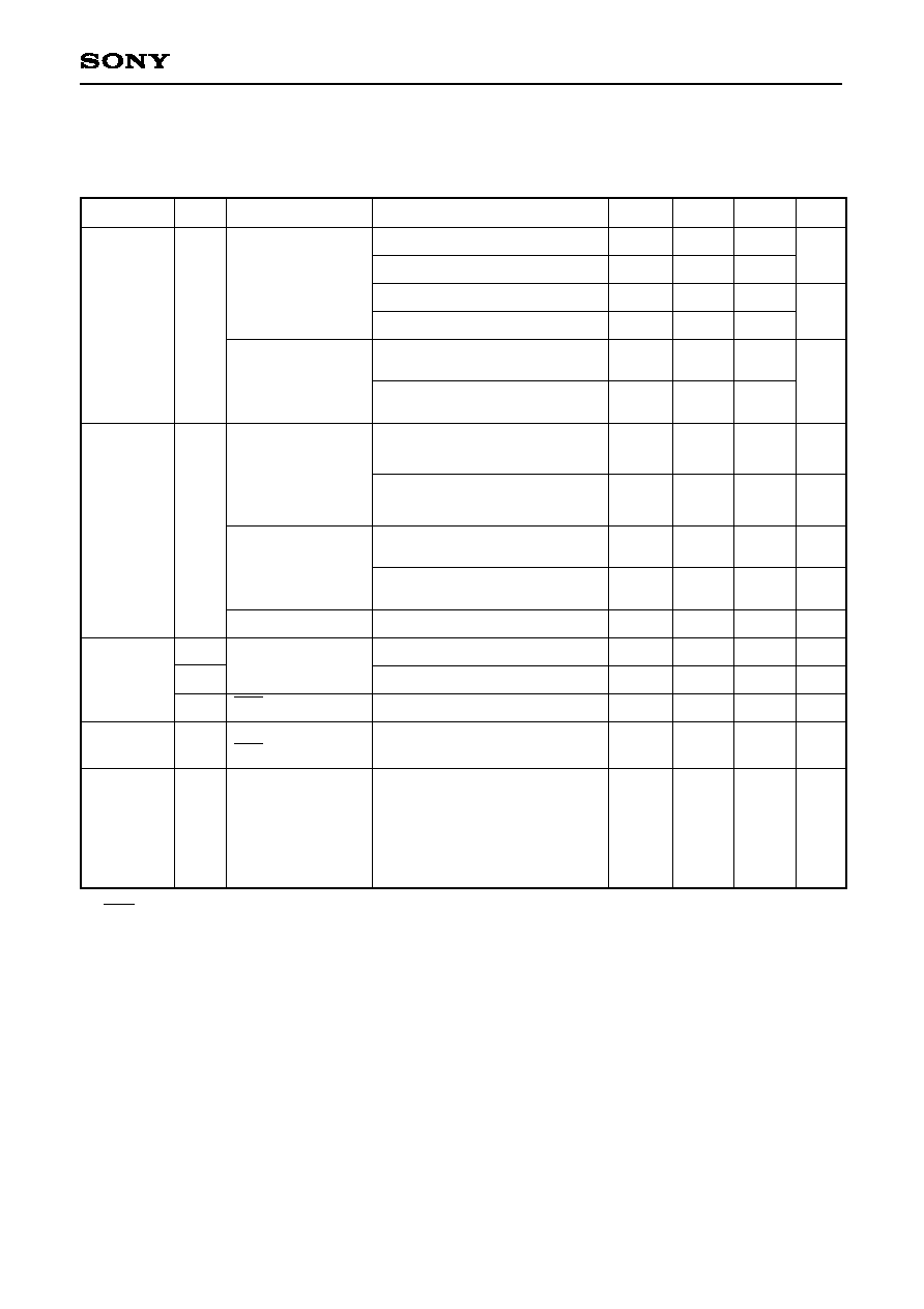
Pin Functions
Symbol
I/O
Functions
PA0/A0
to PA7/A7
PB0/PPO00/
A8
to PB7/PPO07/
A15
PC0/PPO08
to PC3/PPO11
PC4/PPO12/
XCS3
to PC7/PPO15/
XCS0
PD0/D0/
KS12
to PD7/D7/
KS19
PE0/INT0
to PE6/INT6
PE7/INT7/
CINT
PF0/EC0
PF1/EC2
PF2/SCS1/
NMI
PF3/SI1
PF4/SO1
PF5/SCK1
PF6/T1
PF7/T2
PG0/PWM0
to PG1/PWM1
PG2/PWM2
PG3/PWM3
PG4/SCS0
PG5/SI0
PG6/SO0
PG7/SCK0
Output / Output
Output /
Output / Output
I/O / Output
I/O / Output /
Output
I/O / I/O / Input
I/O / Input
I/O / Input /
Input
Input / Input
Input / Input /
Input
Input / Input
Input / Output
Input / I/O
Output / Output
Output / Output
Output / Output
Output / Output
I/O / Input
I/O / Input
I/O / Output
I/O / I/O
(Port A)
8-bit output port.
(8 pins)
(Port B)
8-bit output port. PPO
value and OR output.
(8 pins)
(Port C)
8-bit I/O port. I/O can
be specified in 1-bit
units. PPO value and
OR output.
(8 pins)
(Port D)
8-bit I/O port. I/O can
be specified in 1-bit
units.
(8 pins)
(Port E)
8-bit I/O port. I/O can
be specified in 1-bit
units. (8 pins)
External register interface address bus port
output data value and OR output.
(8 pins)
Programmable pattern generator outputs.
(16 pins)
External register
interface data bus.
(8 pins)
External interrupt inputs.
(8 pins)
External event inputs for 8-bit timer/counter.
(2 pins)
Serial chip select
(CH1) input.
Serial data (CH1) input.
Serial data (CH1) output.
Serial clock (CH1) I/O.
8-bit timer/counter output.
16-bit capture timer/counter timing output.
14-bit PWM output with output value switch
control by programmable pattern generator.
(2 pins)
14-bit PWM output.
(2 pins)
Serial chip select (CH0) input.
Serial data (CH0) input.
Serial data (CH0) output.
Serial clock (CH0) I/O.
External register interface address bus.
Address width can be extended in 1-bit
units.
(8 pins)
External register interface chip select
signal. Chip select signal output function
can be selected in 1-bit units.
(4 pins)
External capture input for 16-bit capture
timer/counter.
Standby release input
function can be
specified in 1-bit units.
(8 pins)
Non-maskable external
interrupt input.
(Port F)
8-bit port. Lower 6 bits
are for input; upper 2
bits are for output.
(8 pins)
(Port G)
8-bit port. Lower 4 bits
are for output; upper 4
bits are for I/O. Upper
4 bits can be specified
in 1-bit units.
(8 pins)
≠ 7 ≠
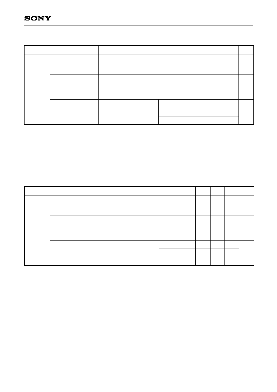
CXP972032/973032/973064
PH0/SDA
PH1/SCL
PH2/RxD
PH3/TxD
PH4/RMC
PH5
PH6/XWR
PH7/XRD
PI0/SCS2
PI1/SI2
PI2/SO2
PI3/SCK2
PI4/AN0/
KS0
to PI7/AN3/
KS3
PJ0/AN4/
KS4
to PJ7/AN11/
KS11
PK0 to PK2
PK3/ADTEN
PK4/ADTRG
PK5
PK6
EXTAL
XTAL
RST
AV
DD
AV
REF
AVss
V
DD
Vss
NC
Output / I/O
Output / I/O
I/O / Input
I/O / Output
I/O / Input
I/O
Output / Output
Output / Output
I/O / Input
I/O / Input
I/O / Output
I/O / I/O
I/O / Input /
Input
I/O / Input /
Input
I/O
I/O / Input
I/O / Input
Output
Input
Input
Input
(Port I)
8-bit I/O port. I/O can
be specified in 1-bit
units.
(8 pins)
(Port J)
8-bit I/O port. I/O can
be specified in 1-bit
units.
(8 pins)
(Port K)
7-bit port. Lower 5 bits
are for I/O; upper 2 bits
are for output. Lower
5 bits can be specified
in 1-bit units.
(7 pins)
Connects a crystal for main clock oscillation. (When the clock is supplied
externally, input it to EXTAL and input an opposite phase clock to XTAL.)
System reset. Active at "L" level.
Positive power supply for A/D converter. (Must be the same voltage with
V
DD
)
Reference voltage input for A/D converter. (Must be the same voltage with
V
DD
)
GND for A/D converter.
Positive power supply.
(Connect both V
DD
pins to positive power supply.)
GND. (Connect all four Vss pins to GND.)
NC. (NC is used for FLASH EEPROM incorporated version.)
I
2
C bus interface data I/O.
I
2
C bus interface clock I/O.
UART reception data input.
UART transmission data output.
Remote control receive circuit input.
External register interface write signal.
External register interface read signal.
Serial chip select (CH2) input.
Serial data (CH2) input.
Serial data (CH2) output.
Serial clock (CH2) I/O.
Analog input for
A/D converter.
(12 pins)
A/D converter operation enable input by external
trigger.
External trigger input for A/D converter.
Standby release input
function can be
specified in 1-bit units.
(12 pins)
Symbol
I/O
Functions
(Port H)
8-bit port. Lower 2 bits
are for large current
N-ch open drain
outputs; medium 4 bits
are for I/O; upper 2 bits
are for output. Medium
4 bits can be specified
in 1-bit units.
(8 pins)
≠ 8 ≠
CXP972032/973032/973064
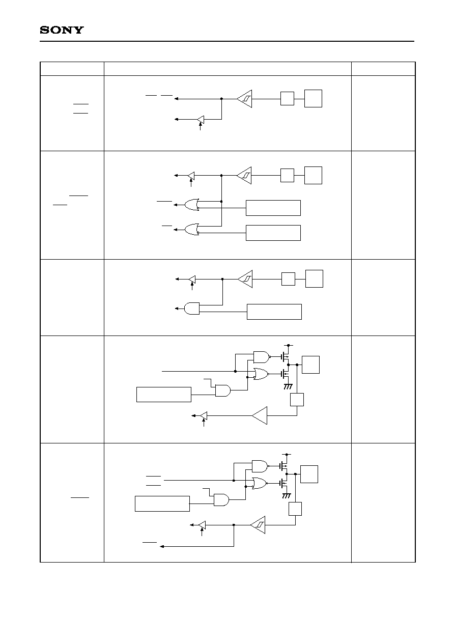
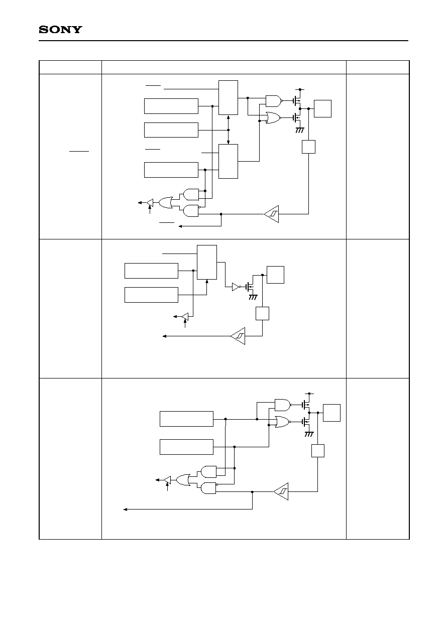
I/O Circuit Format for Pins
Pin
Circuit format
After a reset
PA0/A0
to PA7/A7
Hi-Z
PB0/PPO00/A8
to PB7/PPO07/
A15
Hi-Z
PC0/PPO08
to PC3/PPO11
Hi-Z
A0 to A7
RD
PA register
PA register write
(Undefined after a reset)
Reset
Internal
data bus
Q
S
R
A8 to A15
PPO00 to PPO07
RD
PB register
PB register write
Address width
setting
(Undefined after a reset)
("0" after a reset)
Reset
Internal
data bus
Q
S
R
1
MPX
0
PPO08 to PPO11
RD
PC register
Input
protection
circuit
("0" after a reset)
Internal
data bus
PCD register
("0" after a reset)
IP
≠ 9 ≠
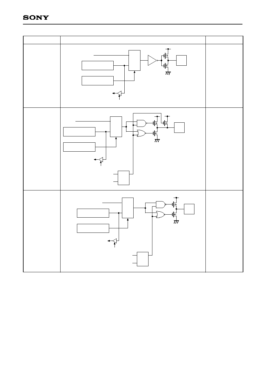
CXP972032/973032/973064
PC4/PPO12/
XCS3
to PC7/PPO15/
XCS0
Hi-Z
PD0/D0/KS12
to PD7/D7/
KS19
Hi-Z
PE0/INT0
to PE7/INT7/
CINT
Hi-Z
XCS3 to XCS0
PPO12 to PPO15
XCS output setting
1
MPX
0
RD
PC register
PCD register
Internal
data bus
("0" after a reset)
("0" after a reset)
("0" after a reset)
IP
RD
PD register
PDD register
External register
I/F
External register
I/F
WR (external register area)
Internal data bus
Internal data bus
Internal data bus
External register operation enable
Standby release
("0" after a reset)
("0" after a reset)
RD (external register area)
External register operation enable
IP
CLR
CLR
Large current drive
5mA (V
DD
= 2.7 to 3.6V)
RD
PE register
PED register
Internal data bus
INT0 to INT7/CINT
(Undefined after a reset)
("0" after a reset)
CMOS Schmitt input
IP
Pin
Circuit format
After a reset
≠ 10 ≠
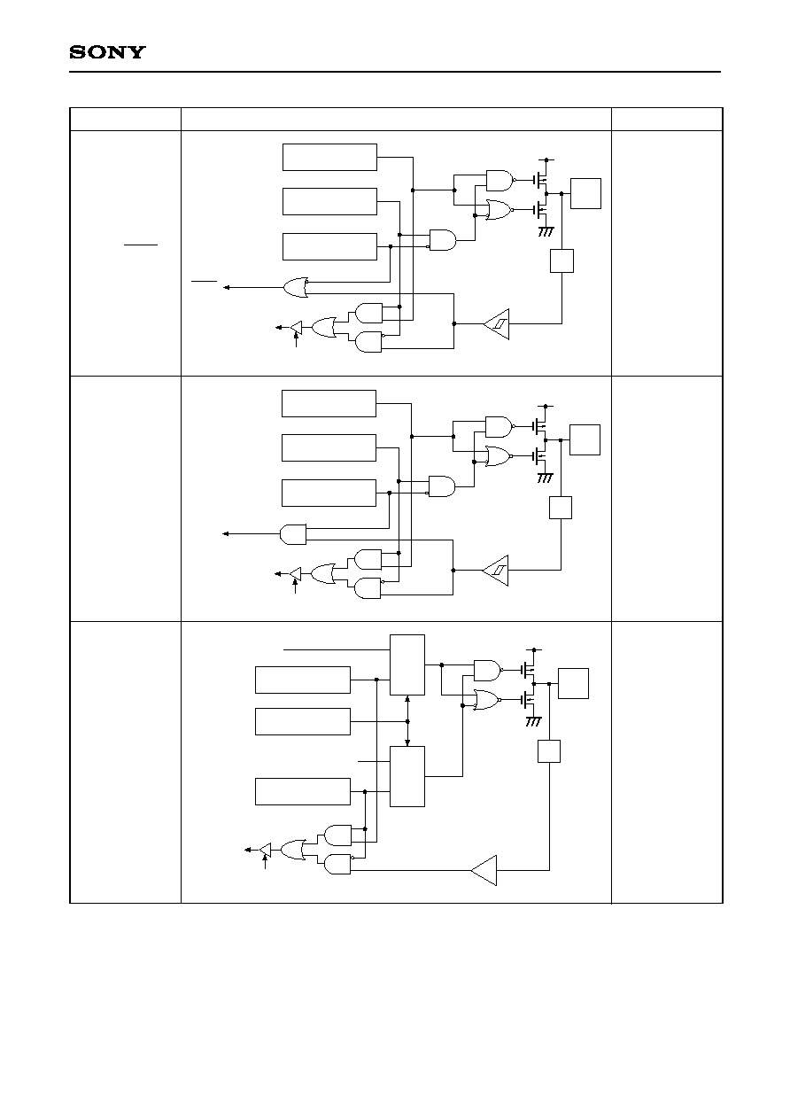
CXP972032/973032/973064
PF0/EC0
PF1/EC2
Hi-Z
PF2/SCS1/
NMI
Hi-Z
PF3/SI1
Hi-Z
PF4/SO1
Hi-Z
PF5/SCK1
Hi-Z
Internal data bus
EC0, EC2
RD
CMOS Schmitt input
IP
PFSL register
("0" after a reset)
NMI input enable
("0" after a reset)
Internal data bus
RD
CMOS Schmitt input
SCS1
NMI
IP
PFSL register
("0" after a reset)
Internal data bus
RD
CMOS Schmitt input
SI1
IP
RD
PFSL register
("0" after a reset)
SO1 output enable
SO1
Internal data bus
IP
RD
CMOS Schmitt input
PFSL register
("0" after a reset)
SCK1 output enable
SCK1
Internal data bus
IP
SCK1
Pin
Circuit format
After a reset
≠ 11 ≠
CXP972032/973032/973064
PF6/T1
"H" level
PF7/T2
"H" level
("H" level at ON
resistance of
pull-up transistor
by a reset.)
PG0/PWM0
to PG3/PWM3
Hi-Z
T1
RD
PFSL register
("1" after a reset)
("0" after a reset)
Internal data bus
1
0
MPX
PF register
PF register write
Reset
Q
S
R
T2
RD
PFSL register
("1" after a reset)
("0" after a reset)
Internal data bus
1
0
MPX
PF register
Pull-up transistor
approximately 150k
(V
DD
= 2.7 to 3.6V)
PG register write
Reset
Q
S
R
PWM0 to PWM3
RD
PGSL register
(Undefined after a reset)
("0" after a reset)
Internal data bus
1
0
MPX
PG register
Pin
Circuit format
After a reset
≠ 12 ≠
CXP972032/973032/973064
PG4/SCS0
Hi-Z
PG5/SI0
Hi-Z
PG6/SO0
Hi-Z
RD
PGD register
PGSL register
Internal data bus
SCS0
("0" after a reset)
PG register
(Undefined after a reset)
("0" after a reset)
IP
CMOS Schmitt input
RD
PGD register
PGSL register
Internal data bus
SI0
("0" after a reset)
PG register
(Undefined after a reset)
("0" after a reset)
IP
CMOS Schmitt input
RD
PG register
PGSL register
Internal
data bus
(Undefined after a reset)
("0" after a reset)
PGD register
("0" after a reset)
SO0 output enable
SO0
IP
1
MPX
0
1
MPX
0
Pin
Circuit format
After a reset
≠ 13 ≠
CXP972032/973032/973064
PG7/SCK0
Hi-Z
PH0/SDA
PH1/SCL
Hi-Z
PH2/RxD
Hi-Z
RD
PG register
PGSL register
Internal
data bus
(Undefined after a reset)
("0" after a reset)
PGD register
("0" after a reset)
SCK0 output enable
CMOS Schmitt input
SCK0
SCK0
IP
1
MPX
0
1
MPX
0
CMOS Schmitt input
RD
PHSL register
Internal data bus
("0" after a reset)
PH register
("1" after a reset)
SDA, SCL
SDA, SCL
IP
1
MPX
0
Large current drive
5mA (V
DD
= 2.7 to 3.6V)
CMOS Schmitt input
RD
PHL register
PHD register
Internal data bus
RxD
(Undefined after a reset)
("0" after a reset)
IP
Pin
Circuit format
After a reset
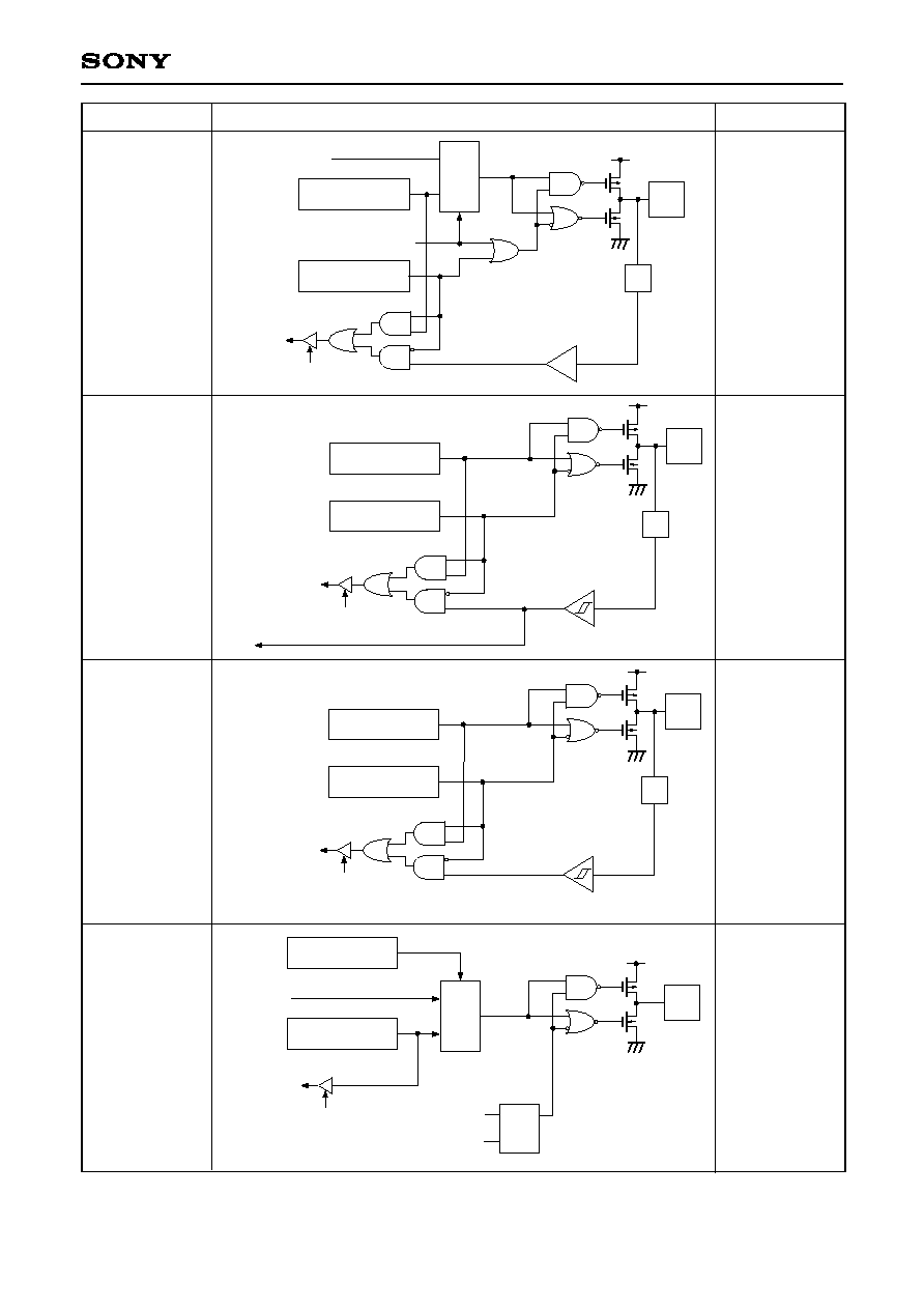
≠ 14 ≠
CXP972032/973032/973064
PH3/TxD
Hi-Z
PH4/RMC
Hi-Z
PH5
Hi-Z
PH6/XWR
PH7/XRD
Hi-Z
RD
PH register
Internal
data bus
(Undefined after a reset)
PHD register
("0" after a reset)
TxD output enable
TxD
IP
1
MPX
0
CMOS Schmitt input
RD
PH register
PHD register
Internal data bus
RMC
(Undefined after a reset)
("0" after a reset)
IP
CMOS Schmitt input
RD
PH register
PHD register
Internal data bus
(Undefined after a reset)
("0" after a reset)
IP
XWR, XRD
RD
PH register
PH register write
PHSL register
(Undefined after a reset)
("0" after a reset)
Reset
Internal
data bus
Q
S
R
1
MPX
0
Pin
Circuit format
After a reset
≠ 15 ≠
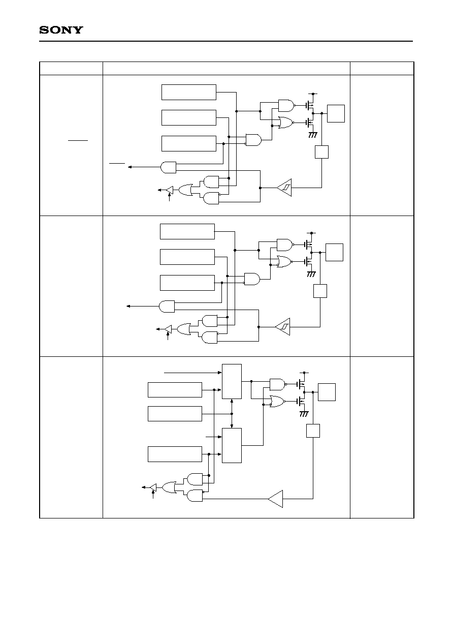
CXP972032/973032/973064
PI0/SCS2
Hi-Z
PI1/SI2
Hi-Z
PI2/SO2
Hi-Z
RD
PID register
PISL register
Internal data bus
SCS2
("0" after a reset)
PI register
(Undefined after a reset)
("0" after a reset)
IP
CMOS Schmitt input
RD
PID register
PISL register
Internal data bus
SI2
("0" after a reset)
PI register
(Undefined after a reset)
("0" after a reset)
IP
CMOS Schmitt input
RD
PI register
PISL register
Internal
data bus
(Undefined after a reset)
("0" after a reset)
PID register
("0" after a reset)
SO2 output enable
SO2
IP
1
MPX
0
1
MPX
0
Pin
Circuit format
After a reset
≠ 16 ≠
CXP972032/973032/973064
PI3/SCK2
Hi-Z
PI4/AN0/KS0
to PI7/AN3/
KS3
Hi-Z
PJ0/AN4/KS4
to PJ7/AN11/
KS11
Hi-Z
RD
PI register
PISL register
Internal data bus
(Undefined after a reset)
("0" after a reset)
PID register
("0" after a reset)
SCK2 output enable
CMOS Schmitt input
SCK2
SCK2
IP
1
MPX
0
1
MPX
0
RD
PID register
PISL register
Internal data bus
Standby release
A/D converter
("0" after a reset)
PI register
(Undefined after a reset)
("0" after a reset)
IP
Input multiplexer
RD
PJD register
PJSL register
Internal data bus
Standby release
A/D converter
("0" after a reset)
PJ register
(Undefined after a reset)
("0" after a reset)
IP
Input multiplexer
Pin
Circuit format
After a reset
≠ 17 ≠
CXP972032/973032/973064
PK0 to PK2
Hi-Z
PK3/ADTEN
PK4/ADTRG
Hi-Z
PK5
"H" level
PK6
"H" level
("H" level at ON
resistance of
pull-up transistor
by a reset.)
RD
PK register
PKD register
Internal data bus
(Undefined after a reset)
("0" after a reset)
IP
RD
PK register
PKD register
Internal data bus
ADTEN, ADTRG
(Undefined after a reset)
("0" after a reset)
CMOS Schmitt input
IP
RD
("1" after a reset)
Internal data bus
PK register
PK register write
Reset
Q
S
R
RD
("1" after a reset)
Internal data bus
PK register
Pull-up transistor
approximately 150k
(V
DD
= 2.7 to 3.6V)
Pin
Circuit format
After a reset
≠ 18 ≠
CXP972032/973032/973064
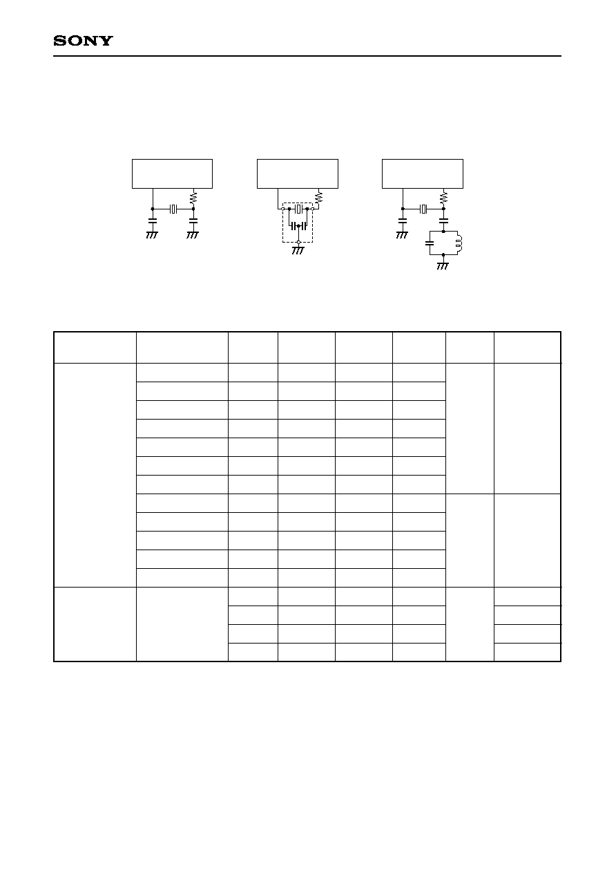
XTAL
EXTAL
Oscillation
RST
"L" level
(during a reset)
Oscillation
stop control
Timing
generator
∑ Diagram shows circuit configuration during oscillation.
∑ Feedback resistor is removed during standby stop mode,
and XTAL is driven at "H" level.
IP
EXTAL
XTAL
Pull-up transistor
approximately 30k
(V
DD
= 2.7 to 3.6V)
IP
RST
Mask option
CMOS Schmitt input
OP
Internal reset circuit
Pin
Circuit format
After a reset
≠ 19 ≠
CXP972032/973032/973064
Absolute Maximum Ratings
(Vss = 0V reference)
Item
Supply voltage
Input voltage
Output voltage
High level output current
High level total output current
Low level output current
Low level total output current
Operating temperature
Storage temperature
Allowable power dissipation
V
DD
AV
DD
AV
REF
AV
SS
V
IN
V
OUT
I
OH
I
OH
I
OL
I
OLC
I
OL
Topr
Tstg
P
D
≠0.3 to +4.6
AV
SS
to +4.6
1
AV
SS
to +4.6
1
≠0.3 to +0.3
≠0.3 to +4.6
2
≠0.3 to +4.6
2
≠5.0
≠50
15.0
20.0
130
≠30 to +85
≠55 to +150
600
380
500
V
V
V
V
V
V
mA
mA
mA
mA
mA
∞C
∞C
mW
Output (value per pin)
Total for all output pins
All pins excluding large
current output pins
(value per pin)
Large current output pins
3
(value per pin)
Total for all output pins
QFP-100P-L01
LQFP-100P-L01
LFLGA-104P-01
Symbol
Rating
Unit
Remarks
1
AV
DD
and AV
REF
must be the same voltage with V
DD
.
2
V
IN
and V
OUT
excluding PH0 and PH1 must not exceed V
DD
+ 0.3V.
3
The large current drive transistor is N-ch transistor of PD and PH0, PH1.
Note) Usage exceeding absolute maximum ratings may permanently impair the LSI. Normal operation should
be conducted under the recommended operating conditions. Exceeding these conditions may adversely
affect the reliability of the LSI.
≠ 20 ≠
CXP972032/973032/973064
Item
Supply voltage
V
DD
AV
DD
AV
REF
V
IH
V
IHS
V
IHEX
V
IL
V
ILS
V
ILEX
Topr
High level input
voltage
Low level input
voltage
Symbol
Min.
2.7
2.0
2.7
2.7
0.7V
DD
0.8V
DD
V
DD
≠ 0.4
0
0
≠0.3
≠30
3.6
3.6
3.6
3.6
V
DD
V
DD
V
DD
+ 0.2
0.2V
DD
0.2V
DD
0.4
+85
V
V
V
V
V
V
V
V
V
∞C
Guaranteed data hold range during stop mode
1
1
2
CMOS Schmitt input
3
EXTAL
4
2
CMOS Schmitt input
3
EXTAL
4
Max.
Unit
Remarks
1
AV
DD
and AV
REF
must be the same voltage with V
DD
.
2
PC, PD, PF4, PG6, PH3, PI2, PI4 to PI7, PJ, PK0 to PK2 for normal input port.
3
RST, PE, PF0 to PF3, PF5, PG4, PG5, PG7, PH0 to PH2, PH4, PH5, PI0, PI1,PI3, PK3 and PK4.
4
Specified only during self-oscillation.
Recommended Operating Conditions
(Vss = 0V reference)
Operating
temperature
≠ 21 ≠
CXP972032/973032/973064
Electrical Characteristics
DC Characteristics 1
(Topr = ≠30 to +85∞C, Vss = 0V reference)
Item
Symbol
Pins
Conditions
Min.
Typ.
Max.
Unit
V
DD
= 3.0V, I
OH
= ≠0.15mA
V
DD
= 2.7V, I
OH
= ≠0.15mA
V
DD
= 3.0V, I
OH
= ≠0.5mA
V
DD
= 2.7V, I
OH
= ≠0.5mA
V
DD
= 3.0V, I
OH
= ≠1.5mA
V
DD
= 2.7V, I
OH
= ≠1.5mA
I
OL
= 1.2mA
I
OL
= 1.6mA
I
OL
= 2.0mA
I
OL
= 3.0mA
I
OL
= 5.0mA
V
DD
= 3.6V, V
IH
= 3.6V
V
DD
= 3.6V, V
IL
= 0.3V
V
DD
= 3.6V, V
IL
= 0.3V
V
DD
= 3.6V, V
I
= 0, 3.6V
V
DD
= 3.6V, V
IH
= 3.6V
V
OH
V
OL
I
IHE
I
ILE
I
ILR
I
IZ
I
LOH
High level
output
voltage
Low level
output
voltage
Input
current
I/O leakage
current
Open drain
output
leakage
current
(N-ch Tr.
off state)
PD to PE, PF6,
PF7, PG0 to PG5,
PH2, PH4, PH5,
PI to PJ,
PK0 to PK6
PA to PC, PF4,
PF5, PG6, PG7,
PH3, PH6, PH7,
PI2, PI3
PE, PF6, PF7,
PG0 to PG5,
PH2, PH4, PH5,
PI0, PI1, PI4 to PI7,
PJ, PK0 to PK6
PA to PC, PF4,
PF5, PG6, PG7,
PH3, PH6, PH7,
PI2, PI3
PD, PH0, PH1
EXTAL
RST
1
PA to PJ, PK0 to PK6,
RST
1
PH0, PH1
2.70
2.40
2.30
2.00
2.30
2.00
0.3
≠0.3
≠0.9
0.30
0.50
0.30
0.50
1.00
61
≠61
≠250
±31
31
V
V
V
V
V
V
V
V
µA
µA
µA
µA
µA
1
RST specifies the input current when pull-up resistor has been selected; the leakage current when no
resistor has been selected.
≠ 22 ≠
CXP972032/973032/973064
Item
Symbol
Pins
Conditions
Min.
Typ.
Max.
Unit
V
DD
= 3.3 ± 0.3V,
f
EX
= fsrc = 40MHz, External clock operation
A/D off state, PLL off state
V
DD
= 3.3 ± 0.3V,
f
EX
= fsrc = 40MHz, External clock operation
A/D off state, PLL off state,
sleep mode
V
DD
= 3.6V, stop mode
2
I
DD1
2
I
DDS2
I
DDS3
Supply
current
1
V
DD
, V
SS
V
DD
, V
SS
V
DD
, V
SS
32
8.0
40
10
25
13
5
mA
mA
µA
DC Characteristics 2 (CXP972032)
(Topr = ≠30 to +85∞C, Vss = 0V reference)
85∞C or less
75∞C or less
50∞C or less
1
When all output pins are open.
2
When the upper two bits (PCK1, PCK0) of the clock control register (CLC: 0002FEh) are set to "00" and the
LSI is operated in high-speed mode (2 frequency dividing clock).
Item
Symbol
Pins
Conditions
Min.
Typ.
Max.
Unit
V
DD
= 3.3 ± 0.3V,
f
EX
= fsrc = 40MHz, External clock operation
A/D off state, PLL off state
V
DD
= 3.3 ± 0.3V,
f
EX
= fsrc = 40MHz, External clock operation
A/D off state, PLL off state,
sleep mode
V
DD
= 3.6V, stop mode
2
I
DD1
2
I
DDS2
I
DDS3
Supply
current
1
V
DD
, V
SS
V
DD
, V
SS
V
DD
, V
SS
35
8.8
44
11
25
13
5
mA
mA
µA
DC Characteristics 2 (CXP973032/973064)
(Topr = ≠30 to +85∞C, Vss = 0V reference)
85∞C or less
75∞C or less
50∞C or less
1
When all output pins are open.
2
When the upper two bits (PCK1, PCK0) of the clock control register (CLC: 0002FEh) are set to "00" and the
LSI is operated in high-speed mode (2 frequency dividing clock).
≠ 23 ≠
CXP972032/973032/973064
Item
Symbol
Pins
Conditions
Min.
Typ.
Max.
Unit
Clock 1MHz,
0V for all pins excluding
measured pins
Clock 1MHz,
0V for all pins excluding
measured pins
Clock 1MHz,
0V for all pins excluding
measured pins
C
IN
C
OUT
C
I/O
Input
capacitance
Output
capacitance
I/O
capacitance
PF0 to PF3,
EXTAL, RST
PA to PB, PF6, PF7,
PG0 to PG3,
PH6, PH7, PK5, PK6,
XTAL
PC to PE, PF4, PF5,
PG4 to PG7,
PH0 to PH5,
PI to PJ, PK0 to PK4
10
10
10
20
20
20
pF
pF
pF
I/O Capacitance
≠ 24 ≠
CXP972032/973032/973064
AC Characteristics
(1) Clock timing
(Topr = ≠30 to +85∞C, V
DD
= 2.7 to 3.6 V, Vss = 0V reference)
Item
Main clock base
oscillation frequency
Main clock base
oscillation input pulse
width
Main clock base
oscillation input
rise time, fall time
Main clock duty
EXTAL,
XTAL
EXTAL,
XTAL
EXTAL,
XTAL
XTAL
Fig.1, Fig.2
Mask option
Selection less than 40MHz
Fig.1, Fig.2
Mask option
Selection less than 20MHz
f
EX
= 40.0MHz
Fig.1, Fig.2
External clock drive
f
EX
= 33.86MHz
Fig.1, Fig.2
External clock drive
f
EX
= 20.0MHz
Fig.1, Fig.2
External clock drive
f
EX
= 40.0MHz
Fig.1, Fig.2
External clock drive
f
EX
= 33.86MHz
Fig.1, Fig.2
External clock drive
f
EX
= 20.0MHz
Fig.1, Fig.2
External clock drive
Fig.1, Fig.2
1/2 V
DD
point
4.76
4.76
4.0
4.0
11
40
40.5
20.5
8.5
10.5
14
60
MHz
MHz
ns
ns
ns
ns
ns
ns
%
Symbol
Pins
Conditions
Min.
Max.
33.86
20.0
50
Typ.
Unit
Note)
t
sys indicates the four values below according to the upper two bits (PCK1, PCK0) of the clock control
register (CLC: 0002FEh).
tsys [ns] = 2/f
EX
(PCK1, PCK0 = 00), 4/f
EX
(PCK1, PCK0 = 01), 8/f
EX
(PCK1, PCK0 = 10),
16/f
EX
(PCK1, PCK0 = 11)
(2) Main clock multiplier circuit
(Topr = ≠30 to +85∞C, V
DD
= 2.7 to 3.6 V, Vss = 0V reference)
f
EX
t
XH
t
XL
t
XH
t
XL
t
XH
t
XL
t
XR
t
XF
t
XR
t
XF
t
XR
t
XF
duty
1
When the degree of input frequency of the main clock base oscillation frequency f
EX
is 10.0 ± 0.1MHz,
quadruple setting is 40.0 ± 0.4MHz.
Note) Main clock multiplier frequency f
SRC
generates the value set from 1.5 times to 4 times of the main clock
base oscillation frequency f
EX
internally according to the Bits 10 to 8 (CMN2 to CMN0) of PLL setting
register (PLL: 0002FCh).
Item
Symbol
Conditions
Min.
Typ.
Max.
Unit
1
≠20 to +85∞C
f
SRC
t
LOCK
Main clock multiplier
frequency
Lock-up time
22.0
19.9
1
40.5
40.5
5
MHz
ms
≠ 25 ≠
CXP972032/973032/973064
EXTAL
XTAL
1/f
EX
t
XH
t
XF
t
XL
t
XR
V
DD
≠ 0.4V
0.4V
XTAL
duty = tx/t
EX
; t
EX
= 1/f
EX
t
EX
t
X
1/2V
DD
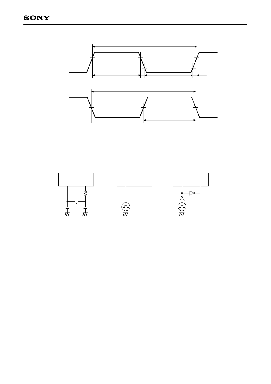
Fig. 2. Oscillator connection and clock applied conditions
EXTAL
XTAL
(iii)
Oscillator connection example
of main oscillation circuit
Connection example (1)
of external clock
Connection example (2)
of external clock
EXTAL
XTAL
(ii)
(i)
EXTAL
XTAL
Fig. 1. Clock timing
≠ 26 ≠
CXP972032/973032/973064
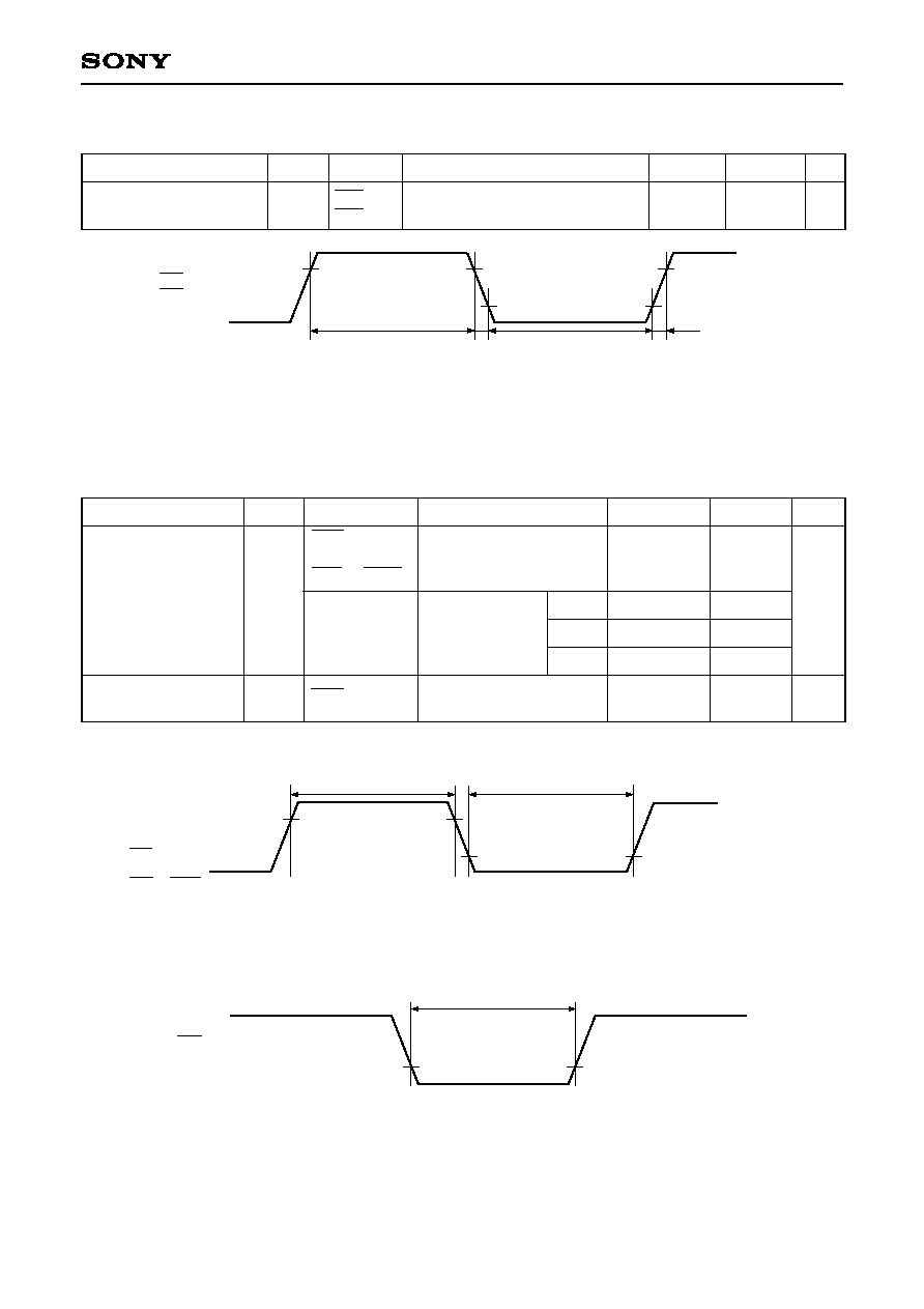
Fig. 3. Event count input timing
EC0
EC2
t
EH
t
EL
0.8V
DD
0.2V
DD
(3) Event count input
(Topr = ≠30 to +85∞C, V
DD
= 2.7 to 3.6V, Vss = 0V reference)
Item
Event count input clock
pulse width
t
EH
,
t
EL
EC0,
EC2
Fig. 3
t
sys + 100
ns
Symbol
Pins
Conditions
Min.
Max.
Unit
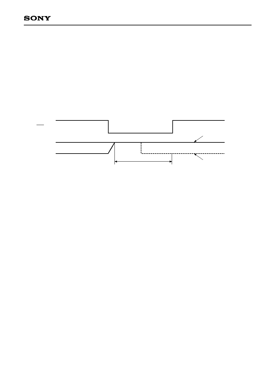
Fig. 4. Interruption input timing
0.2V
DD
t
IH
t
IL
0.8V
DD
NMI
INT0 to INT7
KS0 to KS19
0.2V
DD
RST
t
RST
Fig. 5. Reset input timing
(4) Interruption and reset input
(Topr = ≠30 to +85∞C, V
DD
= 2.7 to 3.6V, Vss = 0V reference)
Item
External interruption
high, low level width
t
IH
,
t
IL
t
RST
NMI,
INT0 to INT7,
KS0 to KS19
INT4 to INT7
RST
Main mode
Sleep mode
Fig. 4
Noise filter
selected
Fig. 4
Fig. 5
PS4
PS6
ns
ns
t
sys + 100
2
t
sys + 100
32/f
EX
+ 100
128/f
EX
+ 100
50/f
EX
Reset input low level
width
Symbol
Pins
Conditions
Min.
Max.
Unit
≠ 27 ≠
CXP972032/973032/973064
Conversion time
Sampling time
Reference input voltage
Analog input voltage
AV
REF
current
t
CONV
t
SAMP
V
REF
I
REF
I
REFS
AV
REF
V
DD
= AV
DD
= AV
REF
= 3.0V
1
1
V
DD
= AV
DD
= AV
REF
Linearity error
Absolute error
Resolution
3.6
AV
REF
2.1
1.7
12
34
t
sys
62
t
sys
10
t
sys
20
t
sys
2.7
0
Main
mode
Item
Symbol
Pins
Conditions
Min.
Typ.
Max.
Unit
Bits
(5) A/D converter characteristics
(Topr = ≠30 to +85∞C, V
DD
= AV
DD
= AV
REF
= 2.7 to 3.6V, Vss = AVss = 0V reference)
8
±1
LSB
LSB
ns
ns
ns
ns
V
V
mA
mA
µA
±3
1.5
1.2
AV
REF
AN0 to AN11
Fig. 6. Definition of A/D converter terms
FFh
FEh
01h
00h
Analog input
Linearity error
Digital conversion value
FFh
(100h)
FEh
01h
00h
Analog input
Digital conversion value
Absolute error
AV
REF
V
FT
2
V
ZT
1
1
V
ZT
: Value at which the digital conversion value changes from 00h to 01h and vice versa.
2
V
FT
: Value at which the digital conversion value changes from FEh to FFh and vice versa.
Absolute error
1
When Bit 6 (ADCK) of A/D control status register (ADCS: 000132h) is specified to "1".
2
When Bit 5 (ADPC) of A/D control status register (ADCS: 000132h) is specified to "1".
Note) AV
DD
and AV
REF
must be the same voltage with V
DD
.
V
DD
= 3.3 ± 0.3V
f
SRC
= 40MHz
V
DD
= 3.3 ± 0.3V
f
SRC
= 20MHz
ADC off state
2
Stop mode
≠ 28 ≠
CXP972032/973032/973064
SCK0,
SCK1,
SCK2
SCK0,
SCK1,
SCK2
SO0,
SO1,
SO2
SCS0,
SCS1,
SCS2
SCS0,
SCS1,
SCS2
SCK0,
SCK1,
SCK2
SCK0,
SCK1,
SCK2
SI0,
SI1,
SI2
SI0,
SI1,
SI2
SO0,
SO1,
SO2
SCK0,
SCK1,
SCK2
Note) The load condition for the SCK output mode and SO output delay time is 100pF.
(6) Serial transfer (CH0, CH1, CH2)
(Topr = ≠30 to +85∞C, V
DD
= 2.7 to 3.6V, Vss = 0V reference)
Item
CS
SCK
delay time
CS
SCK
float delay time
CS
SO
delay time
CS
SO
float delay time
CS high level
width
SCK cycle time
SCK
high, low pulse
width
SI input data
setup time
(for SCK
)
SI input data
hold time
(for SCK
)
SCK
SO
delay time
Minimum interval
time
t
DCSK
t
DSKF
t
DCSO
t
DCSOF
t
WHCS
t
KCY
t
KH
,
t
KL
t
SIK
t
KSI
t
KSO
t
INT
Symbol
Pins
Min.
2
t
sys + 150
2
t
sys + 160
100
110
2
t
sys + 200
2
t
sys + 210
16/f
EX
16/f
EX
t
sys + 100
t
sys + 110
8/f
EX
≠ 100
8/f
EX
≠ 110
100
110
200
210
2
t
sys + 100
2
t
sys + 110
100
110
3
t
sys + 100
3
t
sys + 110
8/f
EX
≠ 100
8/f
EX
≠ 110
ns
ns
ns
ns
ns
ns
ns
ns
ns
ns
ns
ns
ns
ns
ns
ns
ns
ns
ns
ns
ns
ns
ns
ns
Max.
Unit
Conditions
External start
transfer mode
(SCK = output
mode)
External start
transfer mode
Input mode
Output mode
Input mode
Output mode
SCK input mode
SCK output mode
SCK input mode
SCK output mode
SCK input mode
SCK output mode
SCK input mode
SCK output mode
V
DD
= 3.3 ± 0.3V
V
DD
= 3.0 ± 0.3V
V
DD
= 3.3 ± 0.3V
V
DD
= 3.0 ± 0.3V
V
DD
= 3.3 ± 0.3V
V
DD
= 3.0 ± 0.3V
V
DD
= 3.3 ± 0.3V
V
DD
= 3.0 ± 0.3V
V
DD
= 3.3 ± 0.3V
V
DD
= 3.0 ± 0.3V
V
DD
= 3.3 ± 0.3V
V
DD
= 3.0 ± 0.3V
V
DD
= 3.3 ± 0.3V
V
DD
= 3.0 ± 0.3V
V
DD
= 3.3 ± 0.3V
V
DD
= 3.0 ± 0.3V
V
DD
= 3.3 ± 0.3V
V
DD
= 3.0 ± 0.3V
V
DD
= 3.3 ± 0.3V
V
DD
= 3.0 ± 0.3V
V
DD
= 3.3 ± 0.3V
V
DD
= 3.0 ± 0.3V
V
DD
= 3.3 ± 0.3V
V
DD
= 3.0 ± 0.3V
V
DD
= 3.3 ± 0.3V
V
DD
= 3.0 ± 0.3V
V
DD
= 3.3 ± 0.3V
V
DD
= 3.0 ± 0.3V
V
DD
= 3.3 ± 0.3V
V
DD
= 3.0 ± 0.3V
V
DD
= 3.3 ± 0.3V
V
DD
= 3.0 ± 0.3V
V
DD
= 3.3 ± 0.3V
V
DD
= 3.0 ± 0.3V
t
sys + 100
t
sys + 110
1.5
t
sys + 200
1.5
t
sys + 210
1.5
t
sys + 200
1.5
t
sys + 210
1.5
t
sys + 200
1.5
t
sys + 210
1.5
t
sys + 200
1.5
t
sys + 210
ns
ns
ns
ns
ns
ns
ns
ns
ns
ns
≠ 29 ≠
CXP972032/973032/973064
SCK0
SCK1
SCK2
SI0
SI1
SI2
SO0
SO1
SO2
SCS0
SCS1
SCS2
SCK0
SCK1
SCK2
t
INT
0.8V
DD
0.2V
DD
0.8V
DD
t
DCSOF
0.2V
DD
0.8V
DD
t
SIK
t
KSI
0.2V
DD
0.8V
DD
0.2V
DD
0.8V
DD
t
KH
t
DCSKF
t
WHCS
t
KL
t
DCSK
t
KCY
t
KSO
Output data
Input data
t
DCSO
Fig. 7. Serial transfer CH0, CH1, CH2 timing
≠ 30 ≠
CXP972032/973032/973064
1
Due to the total capacitance of the bus.
(7) I
2
C bus
(Topr = ≠30 to +85∞C, V
DD
= 2.7 to 3.6V, Vss = 0V reference)
SCK clock frequency
Bus free time between stop
and start conditions
Hold time under (resend)
start condition
Hold time in SCL clock low
state
Hold time in SCL clock high
state
Setup time under (resend)
start condition
Data hold time
Data setup time
SCL, SDA signal output
rise time
SCL, SDA signal output
fall time
Setup time under stop
condition
SCL
SDA
SDA,
SCL
SCL
SCL
SDA,
SCL
SDA,
SCL
SDA,
SCL
SDA,
SCL
SDA,
SCL
SDA,
SCL
t
SCL
t
BUF
t
HD;STA
t
Low
t
High
t
SU;STA
t
HD;DAT
t
SU;DAT
t
Rd
,
t
Rc
t
Fd
,
t
Fc
t
SU;STO
400
0.9
300
300
1.3
0.6
1.3
0.6
0.6
0
100
20 +
1
20 +
1
0.6
kHz
µs
µs
µs
µs
µs
µs
ns
ns
ns
µs
100
1000
300
4.7
4.0
4.7
4.0
4.7
0
250
4.0
Item
Symbol
Pins
Min.
Standard mode
High-speed mode
Max.
Min.
Max.
Unit
SDA
SCL
t
BUF
t
SU;DAT
t
HD;STA
t
SCL
t
Fd
t
Rd
t
Rc
t
Fc
t
Low
t
HD;STA
t
HD;DAT
t
High
t
SU;STA
t
SU;STO
Fig. 8. I
2
C bus timing
≠ 31 ≠
CXP972032/973032/973064
(8) Remote control reception
(Topr = ≠30 to +85∞C, V
DD
= 2.7 to 3.6V, Vss = 0V reference)
Item
Remote control receive
high, low level width
t
RMC
RMC
Main mode
PS5 selected
PS7 selected
PS9 selected
ns
128/f
EX
+ 100
512/f
EX
+ 100
2048/f
EX
+ 100
Symbol
Pins
Conditions
Typ.
Max.
Unit
0.8V
DD
RMC
0.2V
DD
t
RMC
t
RMC
Fig. 9. Remote control signal input timing
≠ 32 ≠
CXP972032/973032/973064
(9) External register interface
(Vss = 0V reference)
Item
Symbol
Min.
Max.
Min.
Max.
Min.
Max.
3.3 ± 0.3V
Topr = ≠20 to +75∞C
3.3 ± 0.3V
Topr = ≠30 to +85∞C
3.0 ± 0.3V
Topr = ≠30 to +85∞C
Unit
Chip select
pulse width 1
Chip select
pulse width 2
Chip select
pulse width 3
Chip select
pulse width 4
Chip select
pulse width 5
Chip select
pulse width 6
Chip select
pulse width 7
Read/write strobe
pulse width 1
Read/write strobe
pulse width 2
Read/write strobe
pulse width 3
Address setting time 1
Address setting time 2
Address hold time
Read data setting
request time
Read data hold
request time
Write data
setting time 1
Write data
setting time 2
Write data hold time
t
CS1
t
CS2
t
CS3
t
CS4
t
CS5
t
CS6
t
CS7
t
RW1
t
RW2
t
RW3
t
AS1
t
AS2
t
AH
t
DS1
t
DH1
t
DS2
t
DS3
t
DH2
1.5
t
sys
≠20
2.5
t
sys
≠20
2.5
t
sys
≠20
3.5
t
sys
≠20
2.5
t
sys
≠20
3.5
t
sys
≠20
4.5
t
sys
≠20
t
sys ≠ 25
2
t
sys ≠ 25
2
t
sys ≠ 25
t
sys/2
≠25
1.5
t
sys
≠25
t
sys/2
≠25
15
0
1.5
t
sys
≠25
2.5
t
sys
≠25
t
sys/2
≠25
1.5
t
sys
16.5
t
sys
32.5
t
sys
33.5
t
sys
17.5
t
sys
18.5
t
sys
34.5
t
sys
t
sys
16
t
sys
32
t
sys
t
sys/2
1.5
t
sys
--
--
--
1.5
t
sys
16.5
t
sys
t
sys/2
+30
1.5
t
sys
≠20
2.5
t
sys
≠20
2.5
t
sys
≠20
3.5
t
sys
≠20
2.5
t
sys
≠20
3.5
t
sys
≠20
4.5
t
sys
≠20
t
sys ≠ 25
2
t
sys ≠ 25
2
t
sys ≠ 25
t
sys/2
≠25
1.5
t
sys
≠25
t
sys/2
≠25
15
0
1.5
t
sys
≠25
2.5
t
sys
≠25
t
sys/2
≠25
1.5
t
sys
16.5
t
sys
32.5
t
sys
33.5
t
sys
17.5
t
sys
18.5
t
sys
34.5
t
sys
t
sys
16
t
sys
32
t
sys
t
sys/2
1.5
t
sys
--
--
--
1.5
t
sys
16.5
t
sys
t
sys/2
+30
1.5
t
sys
≠30
2.5
t
sys
≠30
2.5
t
sys
≠30
3.5
t
sys
≠30
2.5
t
sys
≠30
3.5
t
sys
≠30
4.5
t
sys
≠30
t
sys ≠ 35
2
t
sys ≠ 35
2
t
sys ≠ 35
t
sys/2
≠35
1.5
t
sys
≠35
t
sys/2
≠35
20
0
1.5
t
sys
≠35
2.5
t
sys
≠35
t
sys/2
≠35
1.5
t
sys
16.5
t
sys
32.5
t
sys
33.5
t
sys
17.5
t
sys
18.5
t
sys
34.5
t
sys
t
sys
16
t
sys
32
t
sys
t
sys/2
1.5
t
sys
--
--
--
1.5
t
sys
16.5
t
sys
t
sys/2
+30
ns
ns
ns
ns
ns
ns
ns
ns
ns
ns
ns
ns
ns
ns
ns
ns
ns
ns
≠ 33 ≠
CXP972032/973032/973064
Read Timing
t1
t
CS1
t
AH
t
AS1
t
RW1
t2
A15 to A0
XCS3 to XCS0
XRD
D7 to D0
t
DS1
t
DH1
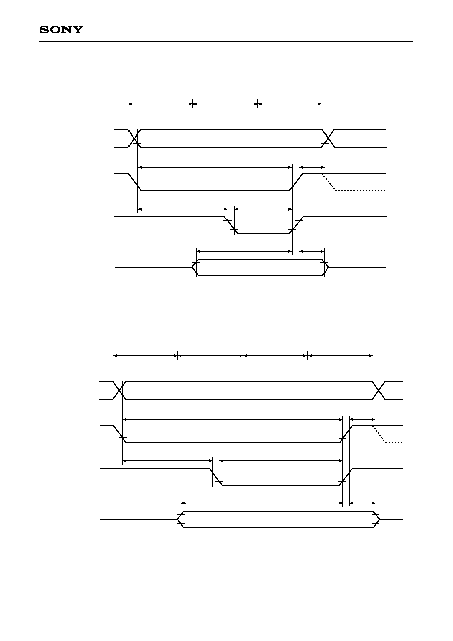
Fig. 10. Byte read (without programmable wait)
t
DS1
t
DH1
t
CS2
t
AH
t
AS1
t
RW2
t1
t2 or tw
t3 or t
W + 1
A15 to A0
XCS3 to XCS0
XRD
D7 to D0
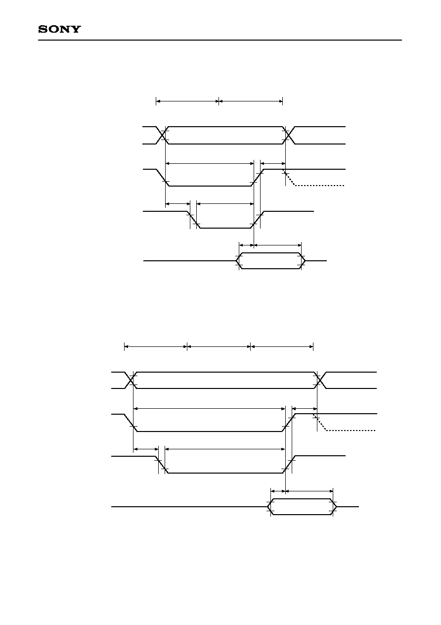
Fig. 11. Byte read (with programmable wait)
≠ 34 ≠
CXP972032/973032/973064
t
DS1
t
DH1
t
CS3
EVEN ADD.
ODD ADD.
t
AH
t
AS1
t
RW3
t1
t2
t3
A15 to A0
XCS3 to XCS0
XRD
D7 to D0
t
DS1
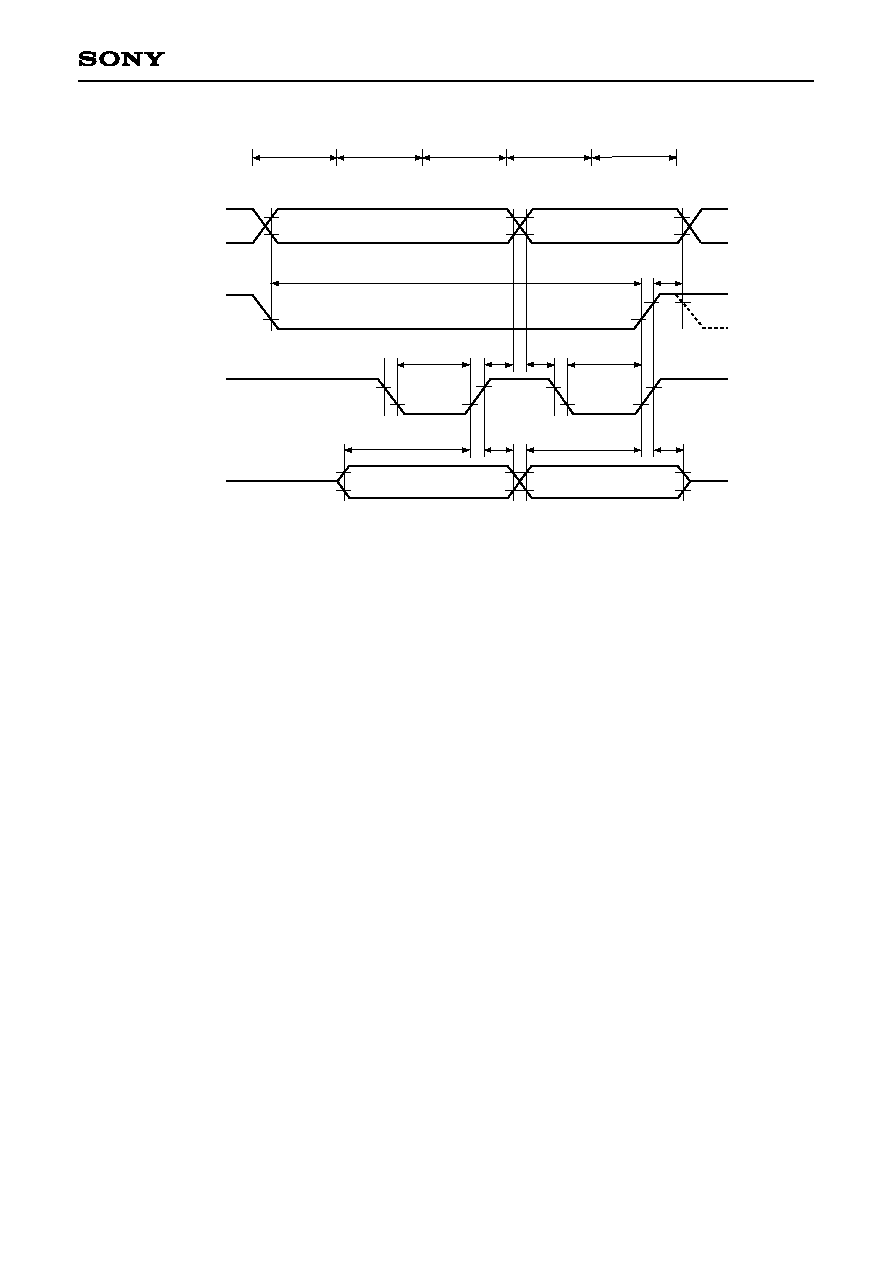
Fig. 12. Word read (no strobe mode, without programmable wait)
t
DS1
t
DH1
t
DH1
t
CS4
EVEN ADD.
ODD ADD.
t
AH
t
AS1
t
AH
t
AS1
t
RW1
t
RW1
t1
t2
t3
t4
A15 to A0
XCS3 to XCS0
XRD
D7 to D0
t
DS1
Fig. 13. Word read (strobe mode, without programmable wait)
≠ 35 ≠
CXP972032/973032/973064
Write Timing
t1
t
CS5
t
AH
t
DS2
t
AS2
t
RW1
t2
t3
A15 to A0
XCS3 to XCS0
XWR
D7 to D0
t
DH2
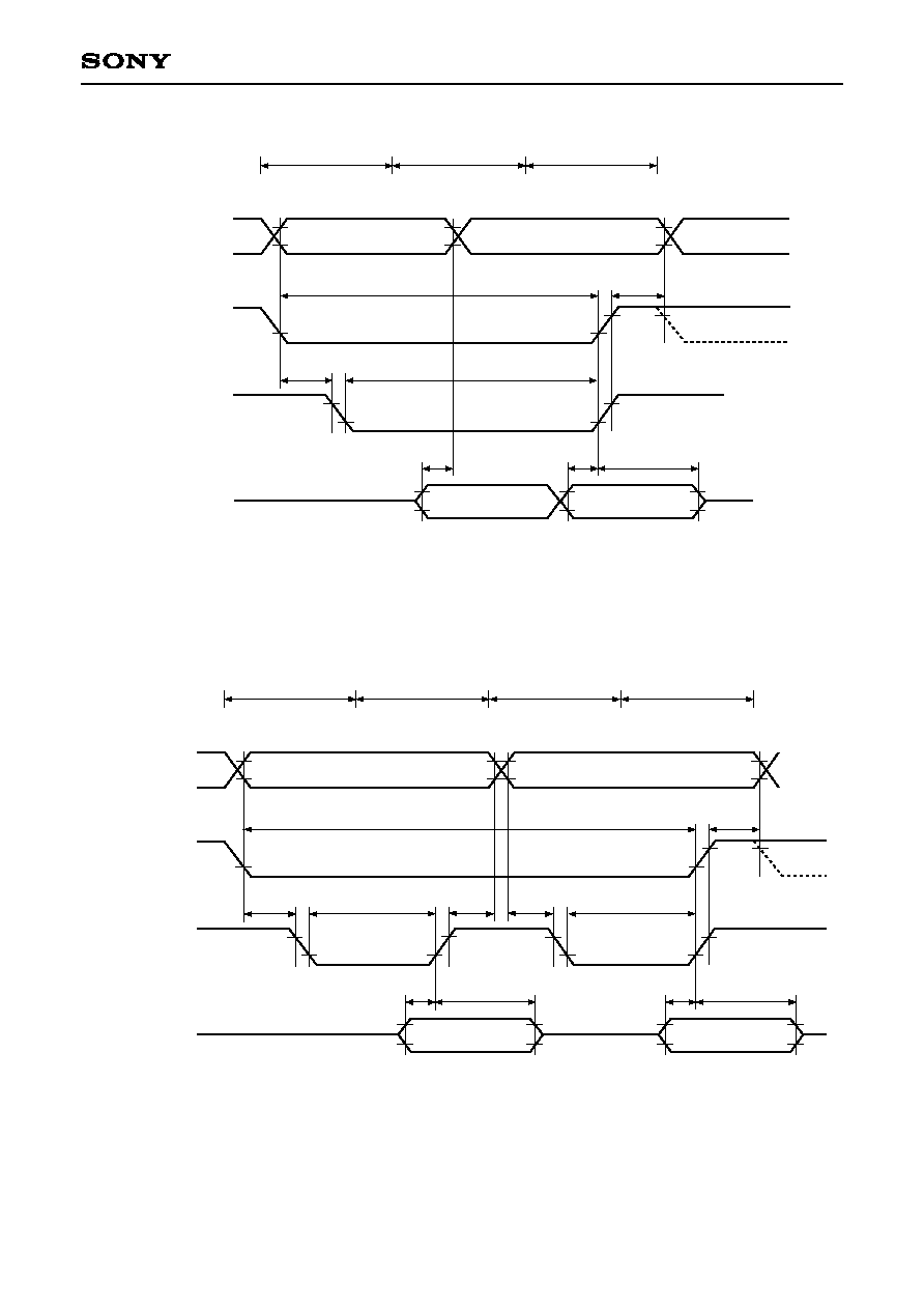
Fig. 14. Byte write (without programmable wait)
t1
t
CS6
t
AH
t
DS3
t
AS2
t
RW2
t2
t3 or tw
t4 or t
W + 1
A15 to A0
XCS3 to XCS0
XWR
D7 to D0
t
DH2
Fig. 15. Byte write (with programmable wait)
≠ 36 ≠
CXP972032/973032/973064
t
DH2
t
CS7
EVEN ADD.
ODD ADD.
t
AH
t
AH
t
AS1
t
RW1
t
RW1
t1
t2
t3
t4
t5
A15 to A0
XCS3 to XCS0
XWR
D7 to D0
t
DS2
t
DH2
t
DS2
Fig. 16. Word write (without programmable wait)
≠ 37 ≠
CXP972032/973032/973064
EXTAL
XTAL
C
1
C
2
Rd
EXTAL
XTAL
C
1
C
2
Rd
EXTAL
(i) Main oscillation circuit
(ii) Main oscillation circuit
(iii) Main oscillation circuit
XTAL
C
1
C
2
Rd
L
C
3
Fig. 17. Recommended oscillation circuit
Appendix
SPC970 Series recommended oscillation circuit and oscillator
MURATA MFG
CO., LTD.
RIVER ELETEC
CO., LTD.
HC-49/U03
CSA6.00MG040
CSA8.00MTZ
CSA10.0MTZ
CSA12.0MTZ
CSA16.00MXZ040
CSA20.00MXZ040
CSA24.00MXZ040
CST6.00MGW040
CST8.00MTW
CST10.0MTW
CST12.0MTW
CST16.00MXW0C3
6.0
8.0
10.0
12.0
16.0
20.0
24.0
6.0
8.0
10.0
12.0
16.0
6.0
8.0
10.0
12.0
100
30
30
30
15
10
7
100
30
30
30
15
18
15
10
10
100
30
30
30
15
10
7
100
30
30
30
15
18
15
10
10
0
0
0
0
0
0
0
0
0
0
0
0
560
330
330
220
(i)
(ii)
Indicates types with on-chip grounding capacitor (C
1
, C
2
).
CL: Load capacitor
(i)
CL = 13.5pF
CL = 12pF
CL = 9.5pF
CL = 10pF
Manufacturer
Model
f
EX
(MHz)
C
1
(pF)
C
2
(pF)
Rd (
)
Circuit
example
Remarks
≠ 38 ≠
CXP972032/973032/973064
Product List
6.0
8.0
10.0
12.0
16.0
20.0
24.0
28.0
32.0
36.0
40.0
6.0
12.0
16.0
28.0
40.0
15
15
10
12
12
12
12
1
3
3
1
36 (±20%)
20 (±20%)
10 (±20%)
10 (±20%)
5
15
15
10
12
12
12
12
1
0.01µF
0.01µF
0.01µF
36 (±20%)
20 (±20%)
10 (±20%)
10 (±20%)
5
5.6k
3.0k
1.8k
1.0k
470
390
200
100
0
0
0
0
0
0
0
0
CL = 16pF
CL = 12pF
(i)
(ii)
(iii)
Indicates types with on-chip grounding capacitor (C
1
, C
2
).
CCR
: Surface mounted type ceramic
oscillator
CL:
Load capacitor
(i)
C3 = 10pF,
L = 2.7µH
C3 = 5pF,
L = 2.7µH
C3 = 3pF,
L = 3.3µH
KINSEKI LTD.
HC-49/U-S
HC-49/U
TDK
Corporation
CCR6.0MC5
CCR12.0MSC5
CCR16.0MSC6
CCR28.0MSC6
CCR40.0MS6
Manufacturer
Model
f
EX
(MHz)
C
1
(pF)
C
2
(pF)
Rd (
)
Circuit
example
Remarks
1
When the main clock base oscillation frequency is specified below 20MH
Z
,
operation is not performed even
though higher external oscillation and higher external input frequency than the upper limit of clock timing
specification are applied.
Type
Product name
ROM capacitance
RAM capacitance
Package
Main clock base
oscillation frequency
1
Reset pin pull-up
resistor
CXP973064
256K byte
11.5K byte
100-pin plastic QFP,
100-pin plastic LQFP,
104-pin plastic LFLGA
Mask ROM
CXP973032
128K byte
11.5K byte
Less than 40MHz,
Less than 20MHz
Existent/Non-existent
CXP972032
128K byte
7.5K byte
100-pin plastic QFP,
100-pin plastic LQFP
≠ 39 ≠
CXP972032/973032/973064
Notes on PK6 Usage
FLASH EEPROM incorporated PK6 is also used as flash mode setting function. Note the followings:
1. "H" is output to PK6 during a reset. That is driven at comparatively high impedance (approximately 150k
),
and take care that V
OH
should not fall under 0.7V
DD
by the partial pressure with external circuit load
impedance.
2. When using software reset functions, PK6 may not rise enough during a reset. Switching PK6 to "H" output
prior to software reset execution or connecting pull-up resistor is recommended.
Mask ROM and piggy/evaluation chip do not have flash mode setting function. Considering that FLASH
EEPROM incorporated version is used, above countermeasure should be performed.
Keep PK6 above 0.7V
DD
during this period.
RST
PK6
Flash mode
Normal operation

≠ 40 ≠
CXP972032/973032/973064
Characteristics Curve (CXP973032/973064)
40
36
32
28
I
DD
≠
Supply current [mA]
24
20
16
12
4
0
2.1
2.4
2.7
V
DD
≠ Supply voltage [V]
I
DD
vs. V
DD
(f
EX
= 40MHz, Topr = 25
∞
C, Typical)
3.3
3
3.6
3.9
8
40
36
32
28
24
I
DD
≠
Supply current [mA]
20
16
12
8
4
2.1
2.4
2.7
3
V
DD
≠ Supply voltage [V]
I
DD
vs. V
DD
(f
EX
= 40MHz, Topr = 25
∞
C, Typical)
3.3
3.6
3.9
0
40
36
32
28
24
I
DD
≠
Supply current [mA]
20
16
12
8
4
0
10
20
f
EX
≠ Main clock base oscillation frequency [MHz]
I
DD
vs. f
EX
(V
DD
= 3V, Topr = 25
∞
C, Typical)
30
40
0
40
36
32
28
24
I
DD
≠
Supply current [mA]
20
16
12
8
4
10
20
f
EX
≠ Main clock base oscillation frequency [MHz]
I
DD
vs. f
EX
(V
DD
= 3V, Topr = 25
∞
C, Typical)
30
40
0
0
Sleep mode
(2 frequency dividing mode)
Sleep mode
(4 frequency dividing mode)
Sleep mode
(8 frequency dividing mode)
Sleep mode
(16 frequency dividing mode)
4 frequency
dividing mode
2 frequency
dividing mode
4 frequency
dividing mode
2 frequency
dividing mode
8 frequency
dividing mode
16 frequency
dividing mode
Sleep mode
(2 frequency dividing mode)
Sleep mode
(4 frequency dividing mode)
Sleep mode
(8 frequency dividing mode)
Sleep mode
(16 frequency dividing mode)
8 frequency
dividing mode
16 frequency
dividing mode
≠ 41 ≠
CXP972032/973032/973064
Characteristics Curve (CXP972032)
40
36
32
28
I
DD
≠
Supply current [mA]
24
20
16
12
4
0
2.1
2.4
2.7
V
DD
≠ Supply voltage [V]
I
DD
vs. V
DD
(f
EX
= 40MHz, Topr = 25
∞
C, Typical)
3.3
3
3.6
3.9
8
40
36
32
28
24
I
DD
≠
Supply current [mA]
20
16
12
8
4
2.1
2.4
2.7
3
V
DD
≠ Supply voltage [V]
I
DD
vs. V
DD
(f
EX
= 40MHz, Topr = 25
∞
C, Typical)
3.3
3.6
3.9
0
40
36
32
28
24
I
DD
≠
Supply current [mA]
20
16
12
8
4
0
10
20
f
EX
≠ Main clock base oscillation frequency [MHz]
I
DD
vs. f
EX
(V
DD
= 3V, Topr = 25
∞
C, Typical)
30
40
0
40
36
32
28
24
I
DD
≠
Supply current [mA]
20
16
12
8
4
10
20
f
EX
≠ Main clock base oscillation frequency [MHz]
I
DD
vs. f
EX
(V
DD
= 3V, Topr = 25
∞
C, Typical)
30
40
0
0
Sleep mode
(2 frequency dividing mode)
Sleep mode
(4 frequency dividing mode)
Sleep mode
(8 frequency dividing mode)
Sleep mode
(16 frequency dividing mode)
4 frequency
dividing mode
2 frequency
dividing mode
Sleep mode
(2 frequency dividing mode)
Sleep mode
(4 frequency dividing mode)
Sleep mode
(8 frequency dividing mode)
Sleep mode
(16 frequency dividing mode)
8 frequency
dividing mode
16 frequency
dividing mode
4 frequency
dividing mode
2 frequency
dividing mode
8 frequency
dividing mode
16 frequency
dividing mode
≠ 42 ≠
CXP972032/973032/973064
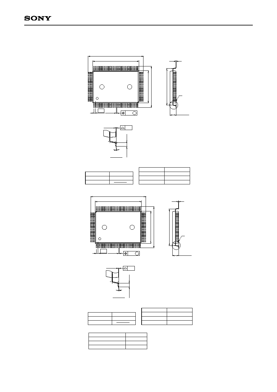
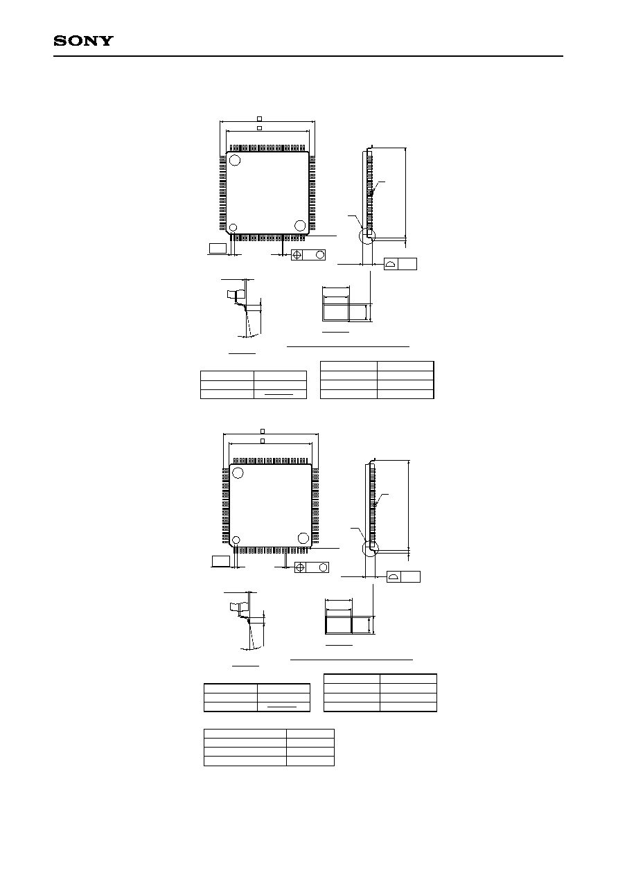
Package Outline
Unit: mm
SONY CODE
EIAJ CODE
JEDEC CODE
PACKAGE MATERIAL
LEAD TREATMENT
LEAD MATERIAL
PACKAGE MASS
EPOXY RESIN
SOLDER PLATING
42/COPPER ALLOY
PACKAGE STRUCTURE
23.9
±
0.4
QFP-100P-L01
100PIN QFP (PLASTIC)
20.0 ≠ 0.1
+ 0.4
0.15 ≠ 0.05
+ 0.1
15.8
±
0.4
17.9
±
0.4
14.0
≠
0.1
+ 0.4
2.75 ≠ 0.15
+ 0.35
A
0.65
M
0.13
QFP100-P-1420
1.7g
1
100
81
80
51
50
31
30
0.3 ≠ 0.1
+ 0.15
DETAIL A
0∞ to 10∞
0.8
±
0.2
(16.3)
0.15
0.1 ≠ 0.05
+ 0.2
LEAD SPECIFICATIONS
ITEM
LEAD MATERIAL
ALLOY 42
LEAD TREATMENT
Sn-Bi 2.5%
LEAD TREATMENT THICKNESS
5-18
µ
m
SPEC.
≠ 43 ≠
CXP972032/973032/973064
Package Outline
Unit: mm
100PIN LQFP (PLASTIC)
25
26
51
50
75
76
1
100
SONY CODE
EIAJ CODE
JEDEC CODE
PACKAGE MATERIAL
LEAD TREATMENT
LEAD MATERIAL
PACKAGE MASS
EPOXY RESIN
SOLDER PLATING
42 / COPPER ALLOY
PACKAGE STRUCTURE
DETAIL A
LQFP-100P-L01
P-LQFP100-14x14-0.5
16.0
±
0.2
14.0
±
0.1
0.5
b
(0.22)
A
1.5 ≠ 0.1
+ 0.2
0.5
±
0.2
(15.0)
0∞ to 10∞
0.1
±
0.1
0.5
±
0.2
0.1
NOTE: Dimension "
" does not include mold protrusion.
0.7g
0.13 M
b = 0.18 ≠ 0.03
( 0.18 )
(0.127)
+ 0.08
0.127 ≠ 0.02
+ 0.05
DETAIL B
B
100PIN LQFP (PLASTIC)
25
26
51
50
75
76
1
100
SONY CODE
EIAJ CODE
JEDEC CODE
PACKAGE MATERIAL
LEAD TREATMENT
LEAD MATERIAL
PACKAGE MASS
EPOXY RESIN
SOLDER PLATING
42 / COPPER ALLOY
PACKAGE STRUCTURE
DETAIL A
LQFP-100P-L01
P-LQFP100-14x14-0.5
16.0
±
0.2
14.0
±
0.1
0.5
b
(0.22)
A
1.5 ≠ 0.1
+ 0.2
0.5
±
0.2
(15.0)
0∞ to 10∞
0.1
±
0.1
0.5
±
0.2
0.1
NOTE: Dimension "
" does not include mold protrusion.
0.7g
0.13 M
b = 0.18 ≠ 0.03
( 0.18 )
(0.127)
+ 0.08
0.127
≠
0.02
+ 0.05
DETAIL B
B
LEAD SPECIFICATIONS
ITEM
LEAD MATERIAL
ALLOY 42
LEAD TREATMENT
Sn-Bi 2.5%
LEAD TREATMENT THICKNESS
5-18
µ
m
SPEC.
≠ 44 ≠
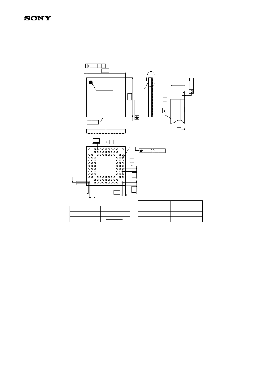
CXP972032/973032/973064
Package Outline
Unit: mm
Sony Corporation
SONY CODE
EIAJ CODE
JEDEC CODE
PACKAGE MASS
PACKAGE STRUCTURE
LFLGA-104P-01
ORGANIC SUBSTRATE
0.3g
PACKAGE MATERIAL
TERMINAL TREATMENT
TERMINAL MATERIAL
GOLD PLATING
NICKEL PLATING
104PIN LFLGA
P-LFLGA104-11x11-0.8
DETAIL X
1.4MAX
S
S
0.20
S
0.10
0.01
X
PIN 1 INDEX
11.0
0.2
A
S
11.0
0.2
B
S
0.15
x4
1 2 3 4 5 6 7 8 9 10111213
103 ≠
0.40 ± 0.05
0.08
M
S A B
A
B
0.8
A
B
C
D
E
F
G
H
J
K
L
M
N
0.7
0.8
0.7
0.4
0.4
1.6
1.6