
September 2003
This document specifies SPANSION
memory products that are now offered by both Advanced Micro Devices and
Fujitsu. Although the document is marked with the name of the company that originally developed the specification,
these products will be offered to customers of both AMD and Fujitsu.
Continuity of Specifications
There is no change to this datasheet as a result of offering the device as a SPANSION
product. Future routine
revisions will occur when appropriate, and changes will be noted in a revision summary.
Continuity of Ordering Part Numbers
AMD and Fujitsu continue to support existing part numbers beginning with "Am" and "MBM". To order these
products, please use only the Ordering Part Numbers listed in this document.
For More Information
Please contact your local AMD or Fujitsu sales office for additional information about SPANSION
memory
solutions.
TM
TM
TM
SPANSION Flash Memory
Data Sheet
TM

DS05-20902-1E
FUJITSU SEMICONDUCTOR
DATA SHEET
FLASH MEMORY
CMOS
64 M (8M
�
�
�
�
8/4M
�
�
�
�
16) BIT
MirrorFlash
TM
*
MBM29PL64LM
90/10
s
s
s
s
DESCRIPTION
The MBM29PL64LM is a 64M-bit, 3.0 V-only Flash memory organized as 8M bytes by 8 bits or 4M words by 16
bits. The MBM29PL64LM is offered in 48-pin, 58-pin TSOP(1) and 80-ball FBGA. The device is designed to be
programmed in-system with the standard 3.0 V V
CC
supply. 12.0 V V
PP
and 5.0 V V
CC
are not required for write
or erase operations. The devices can also be reprogrammed in standard EPROM programmers.
(Continued)
s
PRODUCT LINE UP
s
s
s
s
PACKAGES
* :
MirrorFlash
TM
is a trademark of Fujitsu Limited.
Note
s
:
�
Programming in byte mode
(
�
8
) is prohibited.
�
Programming to the address that already contains data is prohibited
.
(It is mandatory to erase data prior to overprogram on the same address.)
Part No.
MBM29PL64LM
90
10
V
CC
3.0 V to 3.6 V
3.0 V to 3.6 V
Max Address Access Time
90 ns
100 ns
Max CE Access Time
90 ns
100 ns
Max Page Read Access Time
25 ns
30 ns
48-pin plastic TSOP (1)
56-pin plastic TSOP (1)
80-ball plastic FBGA
(FPT-48P-M19)
(FPT-56P-M01)
(BGA-80P-M01)

MBM29PL64LM
90/10
2
(Continued)
The standard MBM29PL64LM offers access times of 90 ns, allowing operation of high-speed microprocessors
without wait states. To eliminate bus contention the devices have separate chip enable (CE), write enable (WE),
and output enable (OE) controls.
The MBM29PL64LM supports command set compatible with JEDEC single-power-supply EEPROMS standard.
Commands are written into the command register. The register contents serve as input to an internal state-
machine which controls the erase and programming circuitry. Write cycles also internally latch addresses and
data needed for the programming and erase operations. Reading data out of the devices is similar to reading
from 5.0 V and 12.0 V Flash or EPROM devices.
The MBM29PL64LM is programmed by executing the program command sequence. This will invoke the Em-
bedded Program Algorithm
TM
which is an internal algorithm that automatically times the program pulse widths
and verifies proper cell margin. Erase is accomplished by executing the erase command sequence. This will
invoke the Embedded Erase Algorithm
TM
which is an internal algorithm that automatically preprograms the array
if it is not already programmed before executing the erase operation. During erase, the device automatically
times the erase pulse widths and verifies proper cell margin.
The device also features a sector erase architecture. The sector mode allows each sector to be erased and
reprogrammed without affecting other sectors. All sectors are erased when shipped from the factory.
The device features single 3.0 V power supply operation for both read and write functions. Internally generated
and regulated voltages are provided for the program and erase operations. A low V
CC
detector automatically
inhibits write operations on the loss of power. The end of program or erase is detected by Data Polling of DQ
7
,
by the Toggle Bit feature on DQ
6
. Once the end of a program or erase cycle has been completed, the devices
internally return to the read mode.
Fujitsu Flash technology combines years of Flash memory manufacturing experience to produce the highest
levels of quality, reliability, and cost effectiveness. The devices electrically erase all bits within a sector simulta-
neously via hot-hole assisted erase. The words are programmed one word at a time using the EPROM program-
ming mechanism of hot electron injection.

MBM29PL64LM
90/10
3
s
s
s
s
FEATURES
� 0.23
�
�
�
�
m Process Technology
� Single 3.0 V read, program and erase
Minimizes system level power requirements
� Industry-standard pinouts
48-pin TSOP (1) (Package suffix: TN - Normal Bend Type)
56-pin TSOP (1) (Package suffix: PCN - Normal Bend Type)
80-ball FBGA(Package suffix: PBT)
� Minimum 100,000 program/erase cycles
� High performance Page mode
Fast 8 bytes / 4 words access capablilty
� Sector erase architecture
128
�
64K byte and 32K word sectors
Any combination of sectors can be concurrently erased. Also supports full chip erase
� HiddenROM
256 bytes / 128 words of HiddenROM, accessible through a "HiddenROM Entry" command sequence
Factory serialized and protected to provide a secure electronic serial number (ESN)
� WP/ACC input pin
At V
IL
, allows protection of first 64K bytes / 32K words sectors, regardless of sector protection/unprotection
status
At V
ACC
, increases program performance
� Embedded Erase
TM
* Algorithms
Automatically pre-programs and erases the chip or any sector
� Embedded Program
TM
* Algorithms
Automatically writes and verifies data at specified address
� Data Polling and Toggle Bit feature for detection of program or erase cycle completion
� Ready/Busy output (RY/BY)
Hardware method for detection of program or erase cycle completion
� Automatic sleep mode
When addresses remain stable, automatically switches themselves to low power mode
� Program Suspend/Resume
Suspends the program operation to allow a read in another address
� Low V
CC
write inhibit
2.5 V
� Erase Suspend/Resume
Suspends the erase operation to allow a read data and/or program in another sector within the same device
� Sector Group Protection
Hardware method disables any combination of sector groups from program or erase operations
� Sector Group Protection Set function by Extended sector protect command
� Fast Programming Function by Extended Command
� Temporary sector group unprotection
Temporary sector group unprotection via the RESET pin
This feature allows code changes in previously locked sectors
� In accordance with CFI (Common Flash Memory Interface)
*
: Embedded Erase
TM
and Embedded Program
TM
are trademarks of Advanced Micro Devices, Inc.
MBM29PL64LM
90/10
4
s
s
s
s
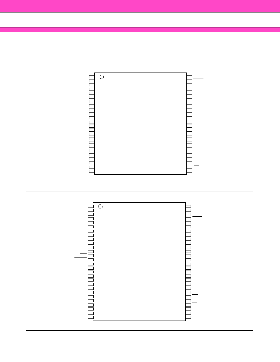
PIN ASSIGNMENTS
A
15
A
14
A
13
A
12
A
11
A
10
A
9
A
8
A
19
A
20
WE
RESET
A
21
WP/ACC
RY/BY
A
18
A
17
A
7
A
6
A
5
A
4
A
3
A
2
A
1
1
2
3
4
5
6
7
8
9
10
11
12
13
14
15
16
17
18
19
20
21
22
23
24
48
47
46
45
44
43
42
41
40
39
38
37
36
35
34
33
32
31
30
29
28
27
26
25
48 pin TSOP(1)
A
16
BYTE
V
SS
DQ
15
/A
-1
DQ
7
DQ
14
DQ
6
DQ
13
DQ
5
DQ
12
DQ
4
V
CC
DQ
11
DQ
3
DQ
10
DQ
2
DQ
9
DQ
1
DQ
8
DQ
0
OE
V
SS
CE
A
0
(Marking Side)
(FPT-48P-M19)
(Top View)
N.C.
N.C.
A
15
A
14
A
13
A
12
A
11
A
10
A
9
A
8
A
19
A
20
WE
RESET
A
21
WP/ACC
RY/BY
A
18
A
17
A
7
A
6
A
5
A
4
A
3
A
2
A
1
N.C.
N.C.
1
2
3
4
5
6
7
8
9
10
11
12
13
14
15
16
17
18
19
20
21
22
23
24
25
26
27
28
56
55
54
53
52
51
50
49
48
47
46
45
44
43
42
41
40
39
38
37
36
35
34
33
32
31
30
29
56 pin TSOP(1)
(Top View)
N.C.
N.C.
A
16
BYTE
V
SS
DQ
15
/A
-1
DQ
7
DQ
14
DQ
6
DQ
13
DQ
5
DQ
12
DQ
4
V
CC
DQ
11
DQ
3
DQ
10
DQ
2
DQ
9
DQ
1
DQ
8
DQ
0
OE
V
SS
CE
A
0
N.C.
V
CCQ
(Marking Side)
(FPT-56P-M01)