 | –≠–ª–µ–∫—Ç—Ä–æ–Ω–Ω—ã–π –∫–æ–º–ø–æ–Ω–µ–Ω—Ç: AD4C111 | –°–∫–∞—á–∞—Ç—å:  PDF PDF  ZIP ZIP |
AD4C111
Dual 1 Form A
Solid State Relay
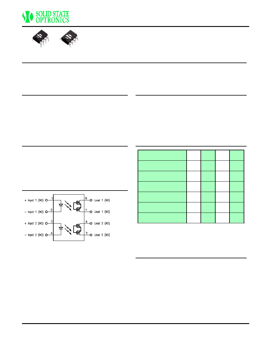
The AD4C111 is a bi-directional, double-pole, single-throw, normally open multipurpose solid-state relay. It is designed to replace
electromechanical relays in general purpose switching applications. The relay consists of two integrated circuits, each driving a pair of
rugged source-to-source enhancement type DMOS transistors. Each integrated circuit is optically coupled to a light emitting diode. The
output MOS transistors are protected with free-wheeling diodes that can handle up to 1.5A of inrush current, making the relay ideal for
switching lamps and highly inductive loads.
DESCRIPTION
FEATURES
APPLICATIONS
OPTIONS/SUFFIXES*
SCHEMATIC DIAGRAM
ABSOLUTE MAXIMUM RATINGS*
APPROVALS
Low input control power consumption (2.5mA TYP)
∑
120mA maximum continuous load current
∑
35 ohms maximum on-resistance
∑
High input-to-output isolation
∑
Long life/high reliability
∑
Reed relay replacement
∑
Meter reading systems
∑
Medical equipment
∑
Battery monitoring
∑
Multiplexers
∑
Surface Mount Option
∑
-S
Tape and Reel Option
∑
-TR
NOTE: Suffixes listed above are not included in marking on
device for part number identification.
PARAMETER
UNIT
MIN
TYP
MAX
Storage Temperature
∞C
-55
125
Operating Temperature
∞C
-40
85
Continuous Input Current
mA
40
Transient Input Current
mA
400
Reverse Input Control
Voltage
V
6
Output Power Dissipation
mW
800
*The values indicated are absolute stress ratings. Functional operation of the
device is not implied at these or any conditions in excess of those defined in
electrical characteristics section of this document. Exposure to Absolute
Ratings may cause permanent damage to the device and may adversely
affect reliability.
BABT CERTIFICATE #607836:
BS EN 60950, BS EN 41003, BS EN 60065
∑
CSA CERTIFICATE #LR111581-1
∑
UL FILE #E90096
∑
© 2004 Solid State Optronics ∑ San JosÈ, CA
www.ssousa.com ∑ +1.408.293.4600
Page 1 of 5
AD4C111
rev 1.40 (10/25/2004)

AD4C111
Dual 1 Form A
Solid State Relay
ELECTRICAL CHARACTERISTICS - 25∞C
PARAMETER
UNIT
MIN
TYP
MAX TEST CONDITIONS
INPUT SPECIFICATIONS
LED Forward Voltage
V
1.2
1.5
If = 10mA
LED Reverse Voltage
V
6
12
Ir = 10uA
Turn-On Current
m
2.5
5
Io = 120mA
A
Turn-Off Current
m
0.5
A
OUTPUT SPECIFICATIONS
Blocking Voltage
V
400
Io = 1uA
Continuous Load Current
m
120
If = 5mA
A
On-Resistance
25
35
Io = 120mA
Leakage Current
µ
0.2
1
Vo = 400V
A
Output Capacitance
p
25
50
Vo = 25V, f = 1.0MHz
F
Offset Voltage
m
0.2
If = 5mA
V
COUPLED SPECIFICATIONS
Isolation Voltage
V
2500
T = 1 minute
-H Suffix
V
3750
T = 1 minute
Turn-On Time
m
0.5
1
If = 5mA, Io = 120mA
s
Turn-Off Time
m
0.1
0.5
If = 5mA, Io = 120mA
s
Isolation Resistance
G
100
Coupled Capacitance
p
3
F
Contact Transient Ratio
V
2000
7000
dV = 50V
/
µ s
© 2004 Solid State Optronics ∑ San JosÈ, CA
www.ssousa.com ∑ +1.408.293.4600
Page 2 of 5
AD4C111
rev 1.40 (10/25/2004)

AD4C111
Dual 1 Form A
Solid State Relay
PERFORMANCE DATA
0
10
20
30
40
50
0.04 0.04 0.05 0.05 0.06 0.06 0.07 0.07
Turn-Off Tim e (m s)
D
e
v
i
c
e
C
ount
AD4C111
Typical Turn-Off Time Distribution
N = 100, Ambient Temperature = 25∞C
0
10
20
30
40
50
16
17
18
19
20
21
22
23
On-Resistance (ohm s)
D
e
v
i
c
e
C
ount
AD4C111
0
20
40
60
80
0.05 0.1 0.15 0.2 0.25 0.3 0.35 0.4
Leakage Current (uA)
D
e
v
i
c
e
C
ount
Typical On-Resistance Distribution
N = 100, Ambient Temperature = 25∞C
AD4C111
Typical Leakage Current Distribution
N = 100, Ambient Temperature = 25∞C
0
10
20
30
40
50
380 400 420 440 460 480 500 520
Blocking Voltage (V)
D
e
v
i
c
e
C
ount
AD4C111
0
50
100
150
-4
0
-2
0
0
20
40
60
80
Tem perature (C)
Loa
d C
u
r
r
e
nt
(
m
A
)
Typical Blocking Voltage Distribution
N = 100, Ambient Temperature = 25∞C
AD4C111
Maximum Load Current vs. Temperature
0
10
20
30
40
0.1
0.2
0.3
0.4
0.5
0.6
0.7
0.8
Turn-On Tim e (m s)
D
e
vi
ce
C
o
u
n
t
AD4C111
Typical Turn-On Time Distribution
N = 100, Ambient Temperature = 25∞C
© 2004 Solid State Optronics ∑ San JosÈ, CA
www.ssousa.com ∑ +1.408.293.4600
Page 3 of 5
AD4C111
rev 1.40 (10/25/2004)
AD4C111
Dual 1 Form A
Solid State Relay
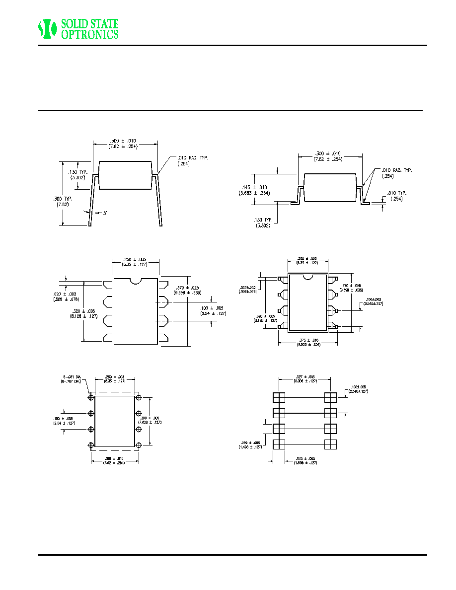
MECHANICAL DIMENSIONS
8 PIN DUAL IN-LINE PACKAGE
8 PIN SURFACE MOUNT DEVICE
END VIEW
END VIEW
TOP VIEW
TOP VIEW
BOTTOM VIEW/
BOARD PATTERN
BOTTOM VIEW/
BOARD PATTERN
© 2004 Solid State Optronics ∑ San JosÈ, CA
www.ssousa.com ∑ +1.408.293.4600
Page 4 of 5
AD4C111
rev 1.40 (10/25/2004)

AD4C111
Dual 1 Form A
Solid State Relay
Solid State Optronics (SSO) makes no warranties or representations with regards to the completeness and accuracy of this document. SSO
reserves the right to make changes to product description, specifications at any time without further notice.
SSO shall not assume any liability arising out of the application or use of any product or circuit described herein. Neither circuit patent
licenses nor indemnity are expressed or implied.
Except as specified in SSO's Standard Terms & Conditions, SSO disclaims liability for consequential or other damage, and we make no other
warranty, expressed or implied, including merchantability and fitness for particular use.
DISCLAIMER
LIFE SUPPORT POLICY
SSO does not authorize use of its devices in life support applications wherein failure or malfunction of a device may lead to personal injury or
death. Users of SSO devices in life support applications assume all risks of such use and agree to indemnify SSO against any and all
damages resulting from such use. Life support devices are defined as devices or systems which, (a) are intended for surgical implant into the
body, or (b) support or sustain life, and (c) whose failure to perform when used properly in accordance with instructions for use can be
reasonably expected to result in significant injury to the user, or (d) a critical component in any component of a life support device or system
whose failure can be reasonably expected to cause failure of the life support device or system, or to affect its safety or effectiveness.
© 2004 Solid State Optronics ∑ San JosÈ, CA
www.ssousa.com ∑ +1.408.293.4600
Page 5 of 5
AD4C111
rev 1.40 (10/25/2004)