 | –≠–ª–µ–∫—Ç—Ä–æ–Ω–Ω—ã–π –∫–æ–º–ø–æ–Ω–µ–Ω—Ç: SSSB138 | –°–∫–∞—á–∞—Ç—å:  PDF PDF  ZIP ZIP |
Swindon Silicon Systems - 1 - July 95
SSSB138
3.0 G Hz Frequency Synthesiser
FEATURES
∑
Very High Speed Operation
∑
Direct Input to Variable Divider
∑
TTL Compatible Program Inputs
∑
ECL 10k Compatible Outputs
∑
50 MHz Phase/Freq Comparator
∑
Small Package 28 pin LCC
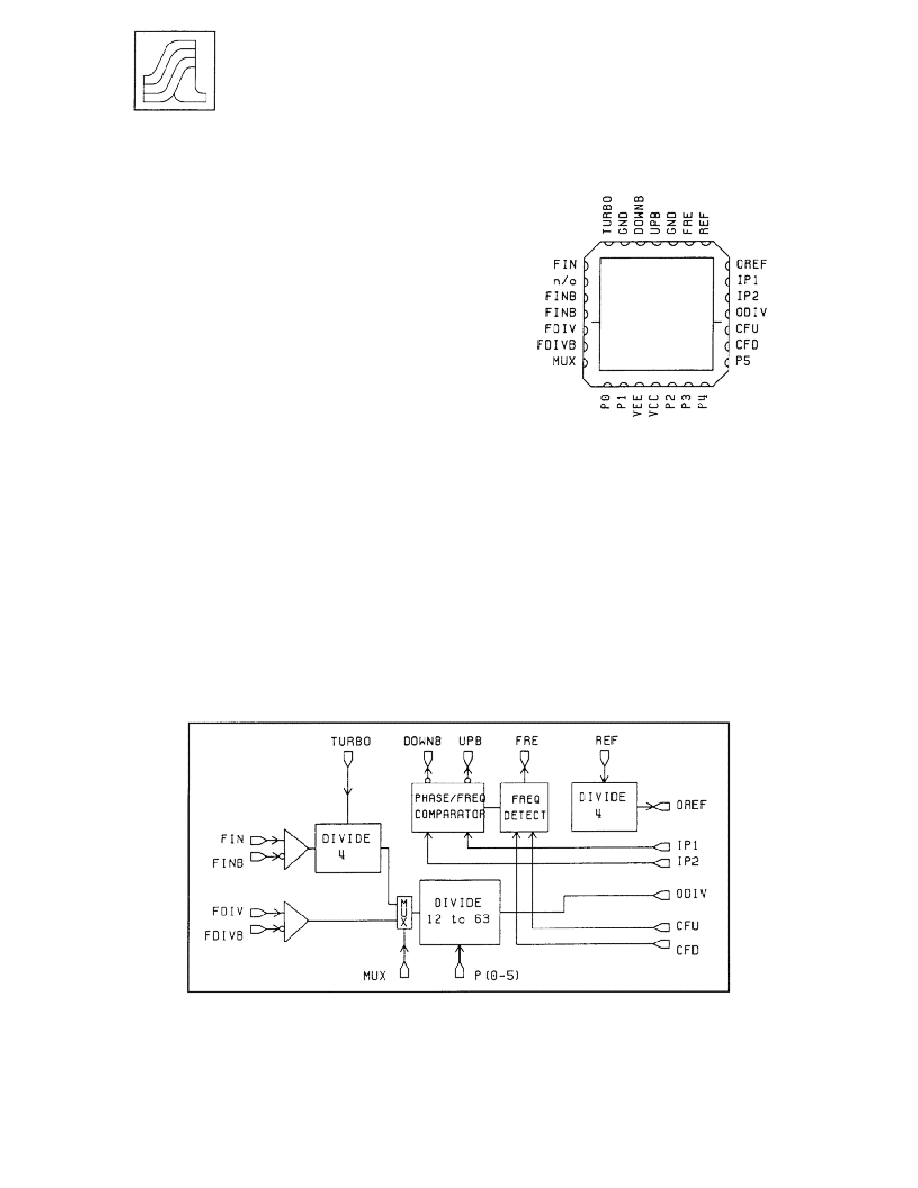
DESCRIPTION
The SSSB138 device has all the digital functions required to produce a high speed phase locked loop: It
contains a high speed divide 4, a divider variable between 12 and 63, a reference divide 4, a
phase/frequency comparator and frequency high low detection circuit. The FIN and FDIV inputs are
internally biased and should be a.c. coupled. The FINB and FDIVB inputs should be decoupled to ground
(Two pins are provided on FINB to reduce series inductance). Control inputs are TTL compatible, and all
other signals are ECL10k compatible. A special high speed mode is selected by the TURBO input for
maximum operating frequency. The variable divider is programmed directly in binary code on the P (0-5)
inputs (note - only codes 12 to 63 should be used). The TURBO input selects on ultra high speed mode for
the high speed divide by 4. This however degrades the low frequency performance, so this input should be
kept low for normal wideband operation. The MUX input selects the clock input source to the variable divider
(FIN via the divide 4 with MUX high, or FDIV with MUX low). The divide 4 is powered down when not
selected.
Block Diagram

Swindon Silicon Systems - 2 - July 95
ELECTRICAL CHARACTERISTICS
Test Conditions (unless otherwise stated) - Tamb = -40∞C to +100∞C Vcc = +5 volts +/- 0.5 volts Vee = -5.2
volts +/- 0.25 volts
PARAMETER
SYM
CONDITIONS
MIN
TYP
MAX
UNITS
Supply Current
Icc
80
105
mA
Iee
85
105
mA
TTL input high voltage VIHT
note 1
2.0
V
TTL input low voltage
VILT
0.8
V
ECL input high voltage VIHE
(Vee =-5.2V)
-1.0
V
ECL input low voltage
VILT
Tamb=25∞C)
-1.58
V
TTL input high current
IIHT
50
uA
TTL input low current
JILT
MUX and RAT
-250
uA
other TTL inputs
-100
uA
ECL input high current IIHE
150
uA
ECL input low current
IILE
40
uA
ECL output high voltage VOHE note 2
-0.93
V
ECL output low voltage VOLE note 2
1.62
V
Max clock frequency -
FIN
FMAX note 3 T = 100∞C
3.0
3.4
GHz
T = 25∞C
3.8
SHz
ODIV phase noise
PNOD note 7
-150
dBc/Hz
Min sinewave freq -
FIN
FMIN
note 4
300
MHz
FDIV max clock freq
FDMX note 5
1.3
GHz
FDIV min sinewave freq FDMN note 5
100
MHz
REF max clock freq
FRMX
200
MHz
REF min sinewave freq FRMN
10
MHz
REF input slew rate
FRSR
10
Wusec
IP1, IP2 max clock rate FCMX
50
MHz
IP1, IP2 min sine freq
FCMN
10
MHz
IP1, IP2 input slew rate FCSR
10
V/usec
Note 1: P(0-5), CFU, CFD, MUX and TURBO are TTL inputs IP1, IP2 and REF are ECL inputs.
(MUX and TURBO have internal pull up resistors to Vcc)
Note 2: Conditions VEE= -5.2V Tamb = 25¯C 100 ohms to - 2.0V.
Note 3: FIN a.c. coupled from 50 ohm source. FINB pins decoupled to ground. Input voltage on FIN 0.6V to
1.0V peak to peak. MUX = 1 and TURBO = 1 (for TURBO = 0 FMAX is reduced by 0.4 GHz).
Higher frequency selections of the device may be available on request.
Note 4: Input voltage on FIN 0.4V to 1.0V pep. MUX = 1 and TURBO = 0 (with TURBO = 1 the SSSB138
operates down to 1.6 GHz).
Note 5: FDIV a.c. coupled from 50 ohm source - FDIVB decoupled to ground.
Input voltage on FDIV 0.4V to 1.0V pep.
Note 6: The SSSB138 device may be operated over its specified frequency range in a suitable Icc socket
(Amphenol - Socapex 49MS028Cy6A socket with 49MV028E19A1 clip) but with some degradation in
dynamic performance.
Note 7: Phase noise at greater than 1KHz from carrier with a 2GHz clock input on FIN.

Swindon Silicon Systems - 3 - July 95
The phase/freq comparator is of the standard MC12044 type but has inverted outputs so that both outputs
are high when 'in lock'. A standard op amp arrangement can be used to generate a VCO drive voltage (see
application circuit). The frequency detector circuit contains a latch which sets when IP1 frequency is greater
than IP2, and resets when IP1 frequency is less than IP2. The inputs CFU and CFD can also be used to set
or reset the latch.
Pin No
Name
Description
1
FINB
High speed clock decoupling pin.
2
FDIV
Variable divider clock input (a.c. coupled)
3
FDIVB
Variable divider clock decoupling pin
4
MUX
High speed Divide 4 select (TTL)
5
P0
Program number LSB (TTL)
6
P1
Program number (TTL)
7
Vee
Negative supply (-5.2V)
8
Vcc
Positive supply (+5.0V)
9-12
P2 - P5
Program number, P5 = MSB
13
CFD
Reset frequency detect
14
CFU
Set frequency detect
15
ODIV
Variable divider output (ECL 10k)
16
IP2
Phase/frequency comparator input (ECL 10k)
17
IP1
Phase/frequency comparator input (ECL 10k)
18
OREF
Reference frequency divide 4 output (ECL 10k)
19
REF
Reference frequency divide 4 input (ECL 10k)
20
FRE
Frequency detect output (ECL 10k)
21
GND
Ground
22
UPB
Phase/frequency comparator output (ECL 10k)
23
DOWNB
Phase/frequency comparator output (ECL 10k)
24
GND
Ground
25
TURBO
High speed mode select (TTL)
26
FIN
High speed clock input (a.c. coupled)
27
N/C
Not connected
28
FINB
High speed clock decoupling pin
Swindon Silicon Systems - 4 - July 95
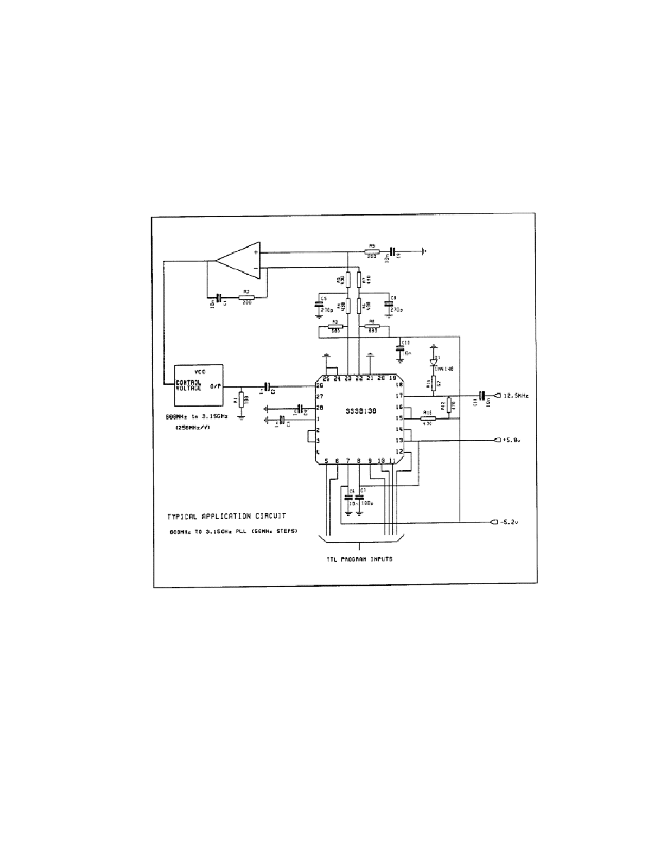
Application Note
The SSSB 138 devices can be used to generate frequencies in the 100MHz to 3GHz range with a phase
locked loop as shown in the application diagram. It should be noted that components used with the device
must be suitable for the frequencies involved, and that lead lengths should be kept as short as possible
particularly for decoupling capacitors.
The fast operating speed of the phase/frequency comparator allows high reference frequencies to be used,
thus increasing potential loop bandwidth. Multi loop techniques can be employed for systems where lower
channel spacings are required. The low phase noise of the high speed ECL circuitry enables such systems
to produce a high spectral purity, low noise signal source with fast frequency hopping capabilities
Swindon Silicon Systems Limited
Radnor Street, Swindon
Wilts SN1 3PR
England
Telephone: 01793 614039
International: +44 1793 614039
Facsimile: 01793 616215
International: +44 1793 616215
This publication is issued to provide outline information only and (unless specifically agreed to the contrary by the
company in writing) is not to be reproduced or to form part of any order or contract or to be regarded as a representation
relating to the products or services concerned. Any applications of product shown in this publication are for illustration
purposes only. We reserve the right to alter without notice the specification, design price or condition of supply of the
product.