
www.SiliconStandard.com 1 of 4
SSM4226M/GM
8/06/2004 Rev.1.02
DUAL N-CHANNEL ENHANCEMENT-MODE POWER MOSFET
Low on-resistance
BV
DSS
30V
Simple drive requirement
R
DS(ON)
18m
High V
GS
rating
I
D
8.2A
Description
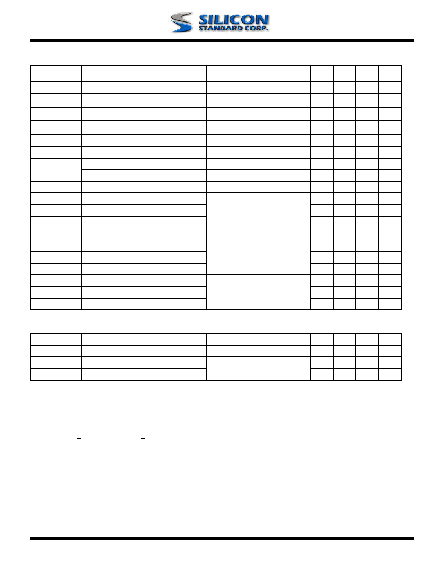
Absolute Maximum Ratings
Symbol
Units
V
DS
V
V
GS
V
I
D
@
T
A
=25
�C
I
D
@
T
A
=70
�C
I
DM
A
P
D
@
T
A
=25
�C
W/
�C
T
STG
T
J
Symbol
Value
Unit
Rthj-a Thermal Resistance Junction-ambient
3
Max. 62.5
�C/W
Parameter
Rating
Drain-Source Voltage
30
Gate-Source Voltage
� 20
Continuous Drain Current
3
8.2
A
Continuous Drain Current
3
6.7
A
Pulsed Drain Current
1
30
Total Power Dissipation 2
W
-55 to 150
�C
Operating Junction Temperature Range -55 to 150
�C
Linear Derating Factor
0.016
Thermal Data
Parameter
Storage Temperature Range
Advanced Power MOSFETs from
Silicon Standard provide the
designer with the best combination of fast switching,
ruggedized device design, ultra low on-resistance and
cost-effectiveness.
G2
D2
S2
G1
D1
S1
S1
G1
S2
G2
D1
D1
D2
D2
SO-8
This device is available with Pb-free lead finish (second-level interconnect) as SSM4226GM.
www.SiliconStandard.com 2 of 4
SSM4226M/GM
8/06/2004 Rev.1.02
Electrical Characteristics
@ T
j
=25
o
C
(unless otherwise specified)
Symbol
Parameter
Test Conditions
Min.
Typ. Max. Units
BV
DSS
Drain-Source Breakdown Voltage
V
GS
=0V, I
D
=250uA
30
-
-
V
B V
DSS
/
T
j
Breakdown Voltage Temperature Coefficient
Reference to 25
�C, I
D
=1mA - 0.03 - V/
�C
R
DS(ON)
Static Drain-Source On-Resistance
2
V
GS
=10V, I
D
=6A - - 18
m
V
GS
=4.5V, I
D
=4A - - 28
m
V
GS(th)
Gate Threshold Voltage
V
DS
=V
GS
, I
D
=250uA
1
-
3
V
g
fs
Forward Transconductance
V
DS
=10V, I
D
=6A
-
15
-
S
I
DSS
Drain-Source Leakage Current (T
j
=25
o
C)
V
DS
=30V, V
GS
=0V
-
-
1
uA
Drain-Source Leakage Current (T
j
=70
o
C)
V
DS
=24V ,V
GS
=0V
-
-
25
uA
I
GSS
Gate-Source Leakage
V
GS
= � 20V
-
-
�100
nA
Q
g
Total Gate Charge
2
I
D
=8A
-
20
30
nC
Q
gs
Gate-Source Charge
V
DS
=24V
-
5
-
nC
Q
gd
Gate-Drain ("Miller") Charge
V
GS
=4.5V
-
12
-
nC
t
d(on)
Turn-on Delay Time
2
V
DS
=15V
-
12
-
ns
t
r
Rise Time I
D
=1A - 8 - ns
t
d(off)
Turn-off Delay Time R
G
=3.3
,
V
GS
=10V - 31 - ns
t
f
Fall Time R
D
=15
-
12
-
ns
C
iss
Input Capacitance
V
GS
=0V
-
1450 2320
pF
C
oss
Output Capacitance
V
DS
=25V
-
320
-
pF
C
rss
Reverse Transfer Capacitance
f=1.0MHz
-
230
-
pF
Source-Drain Diode
Symbol
Parameter
Test Conditions
Min.
Typ. Max. Units
V
SD
Forward On Voltage
2
I
S
=1.7A, V
GS
=0V
-
-
1.2
V
t
rr
Reverse Recovery Time
I
S
=8A,
V
GS
=0
V
,
-
27
-
ns
Q
rr
Reverse Recovery Charge
dI/dt=100A/�s
-
18
-
nC
Notes:
1.Pulse width limited by Max. junction temperature.
2.Pulse width <300us , duty cycle <2%.
3.Surface mounted on 1 in
2
copper pad of
FR4 board ; 135
�C/W when mounted on Min. copper pad.
www.SiliconStandard.com 3 of 4
SSM4226M/GM
8/06/2004 Rev.1.02
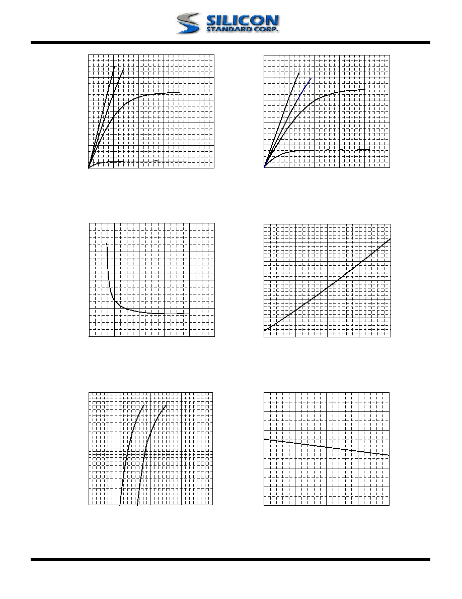
Fig 1. Typical Output Characteristics Fig 2. Typical Output Characteristics
Fig 3. On-Resistance vs. Gate Voltage Fig 4. Normalized On-Resistance
vs. Junction Temperature
Fig 5. Forward Characteristic of Fig 6. Gate Threshold Voltage
Reverse Diode vs. Junction Temperature
0
7
14
21
28
35
0
1
1
2
2
3
V
DS
, Drain-to-Source Voltage (V)
I
D
, Drain Current (A)
T
A
=150
o
C
10V
5.0V
4.0V
V
G
=3.0V
0
7
14
21
28
35
0
1
1
2
2
3
V
DS
, Drain-to-Source Voltage (V)
I
D
, Drain Current (A)
T
A
=25
o
C
10V
5.0V
4.0V
V
G
=3.0V
0.6
0.8
1
1.2
1.4
1.6
1.8
-50
0
50
100
150
T
j
, Junction Temperature (
o
C)
Norm
alize
d R
DS(
ON)
I
D
=6A
V
GS
=10V
0
20
40
60
80
2
4
6
8
10
12
V
GS
, Gate-to-Source Voltage (V)
R
DS
(
ON)
(m
)
I
D
=6.0A
T
A
=25�C
0.1
1
10
0
0.4
0.8
1.2
1.6
V
SD
,Source-to-Drain Voltage (V)
I
S
(A)
T
j
=25
o
C
T
j
=150
o
C
1.00
1.25
1.50
1.75
2.00
2.25
2.50
-50
0
50
100
150
T
j
, Junction Temperature (
o
C )
V
GS(
t
h)
(V)

Information furnished by Silicon Standard Corporation is believed to be accurate and reliable. However, Silicon Standard Corporation makes no
guarantee or warranty, express or implied, as to the reliability, accuracy, timeliness or completeness of such information and assumes no
responsibility for its use, or for infringement of any patent or other intellectual property rights of third parties that may result from its
use. Silicon Standard reserves the right to make changes as it deems necessary to any products described herein for any reason, including
without limitation enhancement in reliability, functionality or design. No license is granted, whether expressly or by implication, in relation to
the use of any products described herein or to the use of any information provided herein, under any patent or other intellectual property rights of
Silicon Standard Corporation or any third parties.
www.SiliconStandard.com 4 of 4
SSM4226M/GM
8/06/2004 Rev.1.02
Fig 7. Gate Charge Characteristics Fig 8. Typical Capacitance Characteristics
10
100
1000
10000
1
5
9
13
17
21
25
29
V
DS
, Drain-to-Source Voltage (V)
C (
p
F)
f=1.0MHz
Ciss
Coss
Crss
0
4
8
12
16
0
10
20
30
40
50
Q
G
, Total Gate Charge (nC)
V
GS
, Gate
to S
o
u
r
c
e
Voltage
(V)
V
DS
=15V
V
DS
=20V
V
DS
=24V
I
D
=8A
0.001
0.01
0.1
1
0.0001
0.001
0.01
0.1
1
10
100
1000
t , Pulse Width (s)
N
o
rmalize
d
The
r
mal Re
sponse
(
R
thja
)
P
DM
Duty factor = t/T
Peak T
j
= P
DM
x R
thja
+ T
a
Rthja = 135
/W
t
T
0.02
0.01
0.05
0.1
0.2
Duty factor=0.5
Single Pulse
0.01
0.1
1
10
100
0.1
1
10
100
V
DS
(V)
I
D
(A)
T
c
=25
o
C
Single Pulse
1s
1ms
10ms
100ms
DC
100us
Fig 9. Maximum Safe Operating Area Fig 10. Effective Transient Thermal Impedance
t
d(on)
t
r
t
d(off)
t
f
V
DS
V
GS
10%
90%
Q
V
G
4.5V
Q
GS
Q
GD
Q
G
Charge
Fig 11. Switching Time Waveform Fig 12. Gate Charge Waveform