 | –≠–ª–µ–∫—Ç—Ä–æ–Ω–Ω—ã–π –∫–æ–º–ø–æ–Ω–µ–Ω—Ç: KU166 | –°–∫–∞—á–∞—Ç—å:  PDF PDF  ZIP ZIP |

27
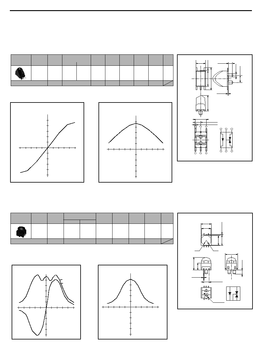
OPTICAL SENSOR
Super intensity infrared LEDs and photo detectors are used in these photo sensors. Stanley offers
high quality and reliability in all of its sensors for use in optical disks, office automation equipment
and optical connectors for surface mount devices.
KU160
Unit
mA
Part No.
DVD
detection output
v
85
270
1.5
50
mV
V
Forward Voltage
MAX.
V
F
Shape
MIN.
MAX.
I
F
fig.
mV
CD
detection output
v
v
c o n d i t i o n : W . D = 2 . 8 m m ( f r o m t h e t o p ) , i n a d e d i c a t e d c i r c u i t
v
P r o d u c t c o n t a i n s n o l e a d
DVD ∑ CD Detecting Sensor
n
Characteristics
n
Package Dimensions
7.7
±
0.5
2
±
0.05
6.5
±
0.1
o
/ 1.5
1.5
±
0.1
11.7
+0
-0.3
+0
-0.1
+0
-0.1
1
9
±
0.1
2.5
±
0.3
0.5
±
0.1
4.3
±
0.5
unit:mm
Ta=25∞C
fig. 3
3
KU165
KU166
Unit
mA
V
Part No. Output voltage
in the liquid
v
V
OH
4.0
0.4
2.0
50
-20~+70
V
V
C
Forward voltage Operating
temperature
MIN.
MAX.
V
F
MAX.
I
F
Topr.
Shape
v
c o n d i t i o n : V c c = 5 V , R
L
= 5 . 6 K
W
, R
L
= V
C E
v a l u e a t R
S
= 1 6 0
W
fig.
Output voltage
in the air
v
V
OL
Liquid Level Detecting Sensor
n
Characteristics
Ta=25∞C
n
Package Dimensions
o
/
9MAX.
11.7
±
0.3
24.7
±
0.3
(o
/
8 Detection depth1.5)
o
/
5Hole
Ditector
die depth
R6.5
7.5
±
0.3
13
±
0.3
7.5
45.2
±
0.3
35.8
±
0.3
4
unit: mm
o
/ 5
±
0.2
1
±
0.2
1.5MAX.
8.6
±
0.2
o
/
5.6
±
0.2
(0.5)
26MIN.
1MIN.
0.7MAX.
0.5
±
0.1
3.2
±
0.2
fig. 1
fig. 2
1
2
28
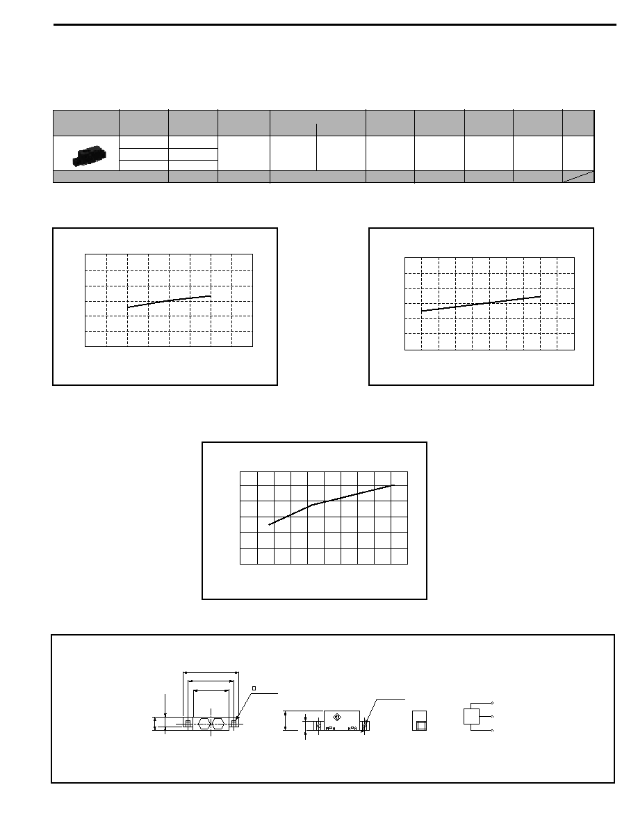
OPTICAL SENSOR
Stanley's optical sensors,KU168 and KU159, can detect the angle of DVD for easy pick-up.
KU168
Unit
±
2.0
24
38
-10~+70
0.62
±
2.5
%
deg.
±
0.1
C
Part No.
sensing
angle
MIN.
v
1
normal absolute
v
1,2
sensitivity
MIN. MAX.
leak output
MAX.
initial freezing
point off set
v
1
operating
temp.
Topr.
fig.
V
Shape
±
0.15
deg.
deg.
deg.
recorded/
not recorded
off set
v
4
reflection rate
off set
v
3,4
v
1 L=7.3mm
v
2 at 1 degree
v
3 RW disk
v
4 aluminum plate mirror is used
v
Product contains no lead
Disk Detecting Sensor (for DVD+RW, DVD-RW, RAM)
n
Characteristics
Ta=25∞C
Output voltage (voltage)
tilt
q
0
-5
+5deg
-100
+100
(A-B)/(A+B)x100
∑ Radial Direction
Output voltage (voltage)
0
-5
+5deg
(A+B)
tilt
q
∑ Tangential Direction
n
Package Dimensions
3
±
0.2
5
±
0.2
5
±
0.2
7
±
0.2
0.5MAX
0.3MAX
2-
o
/
1
2.3
±
0.1
1.2
±
0.1
0.4
±
0.2
1.27
±
0.2
2.54
±
0.2
LED
PD2
PD1
+0
-0.1
4
5
6
6
5
4
3
2
1
1
2
3
unit: mm
fig. 4
4
KU159
Unit
50
2.4
7.2
-10~+70
0.23
±
2
V
deg.
±
0.07
C
Part No.
v
1 derate at
±
2.5 deg.
MAX.
v
1, 2
Leak output
Operating
temperature
MIN.
MAX.
MAX.
v
1
q 0
v
1
Topr.
fig.
deg.
V
%
Shape
Absolute
sensitivity
v
1 c o n d i t i o n : L = 1 0 m m ( F r o m t h e b o t t o m )
v
2 c o n d i t i o n : a t 1 d e g r e e i n a d e d i c a t e d c i r c u i t
v
P r o d u c t c o n t a i n s n o l e a d
Half loading
detection capability
Initial freezing point
off set
Disk Detecting Sensor (for DVD-ROM)
n
Characteristics
n
Package Dimensions
Ta=25∞C
Output voltage (voltage)
tilt
q
0
-5
5V
-5
+5deg
A+B
A-B
Output voltage (voltage)
5V
0
-5
-5
+5deg
(A+B)
tilt
q
6
±
0.2
6
±
0.2
4
±
0.2
7
±
0.2
5.5
±
0.2
2-
o
/ 1.5
LED
PD2
PD1
0.4
±
0.2
2.54
±
0.2
5.5
±
0.2
0.5MAX.
o
/ 6
o
/ 6
2
±
0.2
7.45
±
0.5
0
-0.1
unit: mm
∑ Radial Direction
∑ Tangential Direction
fig. 5
5
29
OPTICAL SENSOR
KU381-40
KU381-60
KU381-80
Unit
400
600
800
5
80
3000
mA
0~+60
350
Open
Collector
(4.7k
W
)
V
msec
5
lx
C
mm
Part No.
Supply Voltage
Vcc
Output
Operating
temperature
Topr.
Mean MAX.
Peak MAX.
I/F
MAX.
Acceptable ambient
illuminate
MAX.
fig.
Shape
v
condition:Vcc=5V, Ambient brightness=0Lux.
Response time
Detection
distance
Current consumption
Human Detecting Sensor
n
Characteristics
29
±
0.2
8
±
0.2
8
±
0.2
11
±
0.2
16.4
±
0.2
37
±
0.2
45
±
0.2
3.2Hole
o
/ 3.2Hole
GND
Vout
Vcc
n
Package Dimensions
Ta=25∞C
1.3
1.1
0.9
0.7
4
4.5
Supply voltage [V]
Relativ
e v
alue of detectab
le r
ange
5
6
5.5
∑ Detection Distance vs. Supply Voltage
0.7
0.9
1.1
1.3
-20
0
20
40
60
80
Ambient Temperature [
C]
Relativ
e v
alue of detectab
le r
ange
∑ Temperature Characteristics
0
0.2
0.4
0.6
0.8
1.0
1.2
0
20
40
60
80
100
reflection rate [%]
Relativ
e v
alue of detectab
le r
ange
∑ Detection Distance vs. Reflection Rate
unit: mm
fig. 6
6

OPTICAL SENSOR
30
KU163A
Unit
90
V
V
Part No.
Photo Current
Rise Time ∑ Fall Time
Forward Voltage
MIN.
V
CE
MAX.
fig.
V
m
s
m
A
Shape
300
688
5
5
2
5
5
10
10
100
5
1.5
5
-30~+85
TYP.
MAX.
I
F
V
CE
I
F
TYP.
V
CE
I
F
R
L
MAX.
I
F
Topr.
mA
V
m
A
mA
mA
W
mA
C
Ip
I
LEAK
tr ∑ tf
V
F
Operating
Temperature
Leak Current
v
Product contains no lead
Reflector Sensor
n
Characteristics
1.9
±
0.1
1.1
±
0.2
(1.9)
photo diode
LED Chip
1
4
2
3
(0.6)
(4.1)
(2.1)
0.45
±
0.2
0.6
±
0.2
2.3
±
0.2
1
2
3
4
3.1
±
0.2
Cathode Mark
n
Package Dimensions
Ta=25∞C
0
1
2
3
4
5
I
F
=5mA
Vce=5V
d=1mm
6
0
0.2
0.4
0.6
0.8
1.0
1.2
1.4
distance [mm]
aluminum mirror
relativ
e v
alue of photo current
90% reflective paper
60% reflective paper
25% reflective paper
18% reflective paper
∑ Detection Range Characteristics
0
10
20
30
40
50
60
70
80
90
100
0
0.2
0.4
0.6
0.8
1.0
1.2
tilt [%]
relativ
e v
alue of photo current
I
F
=5mA
Vce=5V
d=1mm
∑ Detection Distance vs. Object Reflection
0.0
5
10
20
25
30
0.0
2
4
6
LED Current [mA]
relativ
e v
alue of photo current
I
F
=5mA
d=1mm
aluminum evaporated plate
∑ LED Current-Relative Value
-1.5
-1.0
-0.5
0
0.5
0
0.2
0.4
0.6
0.8
1.0
1.2
distance [mm]
relativ
e v
alue of photo current
I
F
=5mA
d=1mm
1.0
1.5
-X
X
∑ Detection Distance Range Characteristics
-1.5
-1.0
-0.5
0
0.5
0
0.2
0.4
0.6
0.8
1.0
1.2
distance [mm]
relativ
e v
alue of photo current
I
F
=5mA
d=1mm
1.0
1.5
-Y
Y
∑ Detection Distance Range Characteristics
Recommended Soldering Pattern
PCB Warpage Direction
unit: mm
fig. 7
(X)
(Y)
7
OPTICAL SENSOR
31
KU167
Unit
V
V
Part No.
INFRARED LED
fig.
mW/cm
2
m
A
Shape
2
4
5
5
TYP.
I
F
mA
V
MH
Z
mA
nA
pF
MAX.
I
F
TYP.
I
F
I
E
V
F
20
1.6
20
12
20
TYP.
V
R
v
2.Ee
I
P
MAX.
V
R
I
D
TYP.
V
R
f
C
T
10
10
3
10
1
Forward Voltage
Cut-Off Frequency
v
1
.f
C
Photo Current
Dark Current
Capacitance
PIN PHOTO DIODE
MH
Z
V
mA
mW/sr
Radiant Intensity
v
1 F c c o n d i t i o n : I
F
= 2 0 m A D C + 1 0 m A p - p
v
2 A s t a n d a r d t u n g s t e n l a m p w i t h c o l o r t e m p e ra t u r e 2 8 5 6 k i s u s e d
v
P r o d u c t c o n t a i n s n o l e a d
Photo Connector
n
Characteristics
2.5
±
0.2
0.9
±
0.2
0.6
±
0.2
1.8
±
0.2
1.5
±
0.2
1
3
2
4
3
±
0.2
photo diode
LED Chip
1
3
2
4
(2.7)
(0.6)
(4.4)
(1)
Cathode Mark
n
Package Dimensions
Ta=25∞C
unit: mm
Recommended Soldering Pattern
PCB Warpage Direction
fig. 9
2.5MAX
14.2
±
0.2
1
±
0.2
5
±
0.2
18
±
0.2
47
±
0.5
22
±
0.2
16.5
±
0.2
6
±
0.2
8
±
0.2
15
±
0.3
APC
R1
.6
2-
C
0.5
R3.
1
o
/
3.2
±
0.2
o
/ 6.2
±
0.2
5
1
5
1
3
2
4
Vout
Vcc
GND
Vmon
GLed
n
Package Dimensions
KUA0003A
Unit
0 ~ +5.5
100
3.9 ~ 4.1
0.2 ~ 0.4
0.9 ~ 4.1
10
mA
msec
±
15
%
Part No.
Supply Voltage
Vcc
Forward
Current
If
Output
Change Rate
v
1
fig
Detector Board A
Detector Board B
Vmon
Tout
V
V
V
V
Shape
Sensor Output
Vout
Response Time
tr ∑ tf
Monitor Output
v
1 O u t p u t c h a n g e ra t e w i t h i n t h e o p e ra t i n g t e m p e ra t u r e ( 0 ~ 6 0
C )
Color Toner Density Sensor
n
Characteristics
Ta=25∞C
unit: mm
fig. 8
8
9