Dual-Line ESD Protection Array STE0512
Working voltage 5V
DESCRIPTION
The STE0512 are designed by TVS device that is to protect sensitive electronics from
damage or latch-up due to ESD. They are designed for use in applications where board space
ia at a premium.
STE0512 will protect up to two lines, and may be used on lines where the signal polarities
swing above and below ground.
STE0512 offer desirable characteristics for board level protection including fast response
time, low operating and clamping voltage without device degradation.
STE0512 may be used to meet the immunity requirements of IEC 61000-4-2, level 4. The
small SOT-523 package makes them ideal for use in portable electronics such as cell phone,
PDA's, notebook computers, digital cameras and MP3.
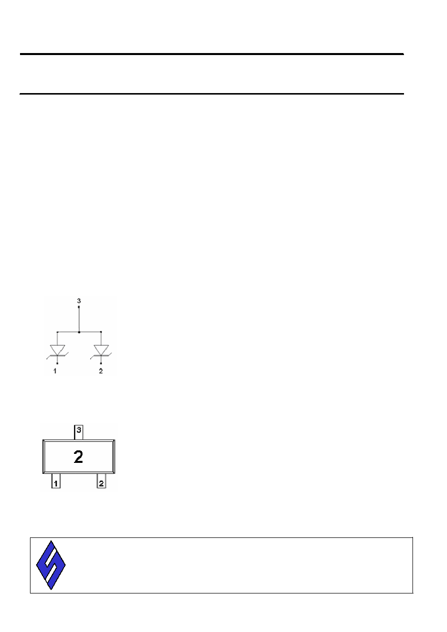
PIN CONFIGURATION
SOT-523
PART MARKING
Page 1
STANSON TECHNOLOGY
120 Bentley Square, Mountain View, Ca 94040 USA
TEL: (650) 9389294 FAX: (650) 9389295
FEATURE
l
Transient protection for data lines to
IEC 61000-4-2 (ESD) +/- 15kV (air),
+/-8KV (contect)
IEC 61000-4-4 (EFT) 40A (5/50ns)
l
Protects two I/O lines
l
Working voltage : 5V
l
Low leakage current
l
Low operating and clamping voltages

Dual
-Line ESD Protection Array STE0512
Working voltage 5V
OREDRING INFORMATION
Part Number
Package
STE0512D52RG
SOT-523
STE0512D52RG: Tape Reel; Pb-Free
ABSOULTE MAXIMUM RATINGS (Ta = 25 Unless otherwise noted )
Parameter
Symbol
Typical
Unit
Peak Pulse Power (tp=8/20 us)
Ppk
250
W
Maximum Peak Pulse Currint (tp=8/20us)
Ipp
7
A
ESD per ICE 61000-4-2 (Air)
Vpp
+/-15
KV
ESD per ICE 61000-4-2 (Contact)
Vpp
+/-8
KV
Operating Junction Tempreature
Tj
-55~150
Storgae Temperature Range
T
STG
-55~150
Lead Soldering Temperature
T
L
260(10sec)
ELECTRICAL CHARACTERISTICS (Ta = 25 Unless otherwise noted )
Parameter
Symbol Conditions
Min Typ Max Unit
Reverse Stand-Off Voltage
V
RWM
5 V
Reverse Breakdown Voltage
V
BR
It=1mA
6
8.5 V
Reverse Leakage Current
I
R
V
RWM
=5V, T=25
0.01 1 uA
Reverse Leakage Current
I
R
V
RWM
=3V, T=25
0.01 0.5 uA
Clamping Voltage
V
C
Ipp=1A, tp=8/20us
11.5 V
Clamping Voltage
V
C
Ipp=7A, tp=8/20us
15 V
Junction Capacitance
Cj
Between I/O Pin and GND
V
R
=0V, f 1MHz
20 30 pF
Page 2
STANSON TECHNOLOGY
120 Bentley Square, Mountain View, Ca 94040 USA
TEL: (650) 9389294 FAX: (650) 9389295

Dual-Line ESD Protection Array STE0512
Working voltage 5V
TYPICAL CHARACTERISTICS
Page 3
STANSON TECHNOLOGY
120 Bentley Square, Mountain View, Ca 94040 USA
TEL: (650) 9389294 FAX: (650) 9389295

Dual-
Line ESD Protection Array STE0512
Working voltage 5V
APPLICATION NOTE
Device Connection for Protection of Two Data Lines
STE0512 is designed to protect up to two data lines. The device is connected as follows:
1.
The TVS protection of two I/O lines is achieved by connecting pins 1,2 to the data lines.
Pin 3 is connected to ground. The ground connection should be made directly to the
ground plane for best results. The path length is kept as short as possible to reduce the
effects of parasitic inductance.
Circuit Board Layout Recommendations for Suppression of ESD
Good circuit board layout is critical for the suppression of ESD induced transients. The
following guidelines are recommended:
1. Place the TVS near the input terminals or connectors to restrict transient coupling.
2. Minimize the path length between the TVS and the protected line.
3. Minimize all conductive loops including power and ground loops.
4. The ESD transient return path to ground should be kept as short as possible.
5. Never run critical signals near board edges
6. Use ground planes whenever possible.
Psgr 4
STANSON TECHNOLOGY
120 Bentley Square, Mountain View, Ca 94040 USA
TEL: (650) 9389294 FAX: (650) 9389295

Dual-Line ESD Protection Array STE0512
Working voltage 5V
SOT-523 PACKAGE OUTLINE
Page 5
STANSON TECHNOLOGY
120 Bentley Square, Mountain View, Ca 94040 USA
TEL: (650) 9389294 FAX: (650) 9389295