STATEK CORPORATION 512 N. MAIN ST., ORANGE, CA 92868 714-639-7810 FAX: 714-997-1256 www.statek.com
DESCRIPTION
The CX-1-SM quartz crystals are leadless devices designed
for surface mounting on printed circuit boards or hybrid
substrates. They are hermetically sealed in a rugged,
miniature ceramic package. The CX-1-SM crystal is
manufactured using the STATEK-developed photo-
lithographic process, and was designed utilizing the
experience acquired by producing millions of crystals for
industrial, commercial, military and medical applications.
Maximum process temperature should not exceed 260
O
C.
FEATURES
Extensional mode
Ideal for use with microprocessors
Designed for low power applications
Compatible with hybrid or PC board packaging
Low aging
Full military testing available
Ideal for battery operated applications
Designed and manufactured in the USA
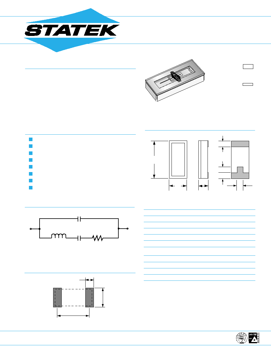
CX-1-SM CRYSTAL
530 kHz to 2.1 MHz
Low Profile, Miniature Surface Mount Quartz Crystal
TM
TYP.
MAX.
DIM
INCHES
mm
INCHES
mm
A
.315
8.00
.330
8.38
B
.140
3.56
.155
3.94
C
-
-
see below
D
.045
1.14
.055
1.40
E
.060
1.52
.070
1.78
DIM "C"
GLASS LID
CERAMIC LID
MAX
INCHES
mm
INCHES
mm
SM1
.065
1.65
.O7O
1.78
SM2
.067
1.70
.072
1.83
SM3
.070
1.78
.075
1.90
10129 - Rev A
A
B
E
D
D
TOP
BOTTOM
C
E
PACKAGE DIMENSIONS
actual size
side view
C
0
C
1
R
1
2
1
L
1
EQUIVALENT CIRCUIT
R
1
Motional Resistance L
1
Motional Inductance
C
1
Motional Capacitance C
0
Shunt Capacitance
.160[4.06]
INCHES[mm]
.070[1.78]
.270[6.86]
SUGGESTED LAND PATTERN

STATEK CORPORATION 512 N. MAIN ST., ORANGE, CA 92868 714-639-7810 FAX: 714-997-1256 www.statek.com
TYPICAL APPLICATION
FOR A PIERCE OSCILLATOR
The low profile CX miniature surface mount crystal is ideal
for small, high density, battery operated portable products.
The CX crystal designed in a Pierce oscillator (single
inverter) circuit provides very low current consumption and
high stability. A conventional CMOS Pierce oscillator circuit
is shown below. The crystal is effectively inductive and in a
PI-network circuit with C
D
and C
G
provides the additional
phase shift necessary to sustain oscillation. The oscillation
frequency (f
O
) is 15 to 150 ppm above the crystal's series
resonant frequency (f
s
).
Drive Level
R
A
is used to limit the crystal's drive level by forming a
voltage divider between R
A
and C
D
. R
A
also stabilizes the
oscillator against changes in the amplifiers output
resistance (R
0
). R
A
should be increased for higher voltage
operation.
Load Capacitance
The CX crystal calibration tolerance is influenced by the
effective circuit capacitances, specified as the load
capacitance (C
L
). C
L
is approximately equal to:
NOTE: C
D
and C
G
include stray layout to ground and C
s
is the stray shunt capacitance between the crystal
terminal. In practice, the effective value of C
L
will be less
than that calculated from C
D
, C
G
and C
S
values because
of the effect of the amplifier output resistance. C
S
should
be minimized.
The oscillation frequency (f
O
) is approximately equal to:
AMPLIFIER
BUFFER
C
G
C
D
R
A
CX-1
Contact factory for
design guidelines
OSC
Freq (f )
O
R
f
C
S
10129 - Rev A
SPECIFICATIONS
Specifications are typical at 25oC unless otherwise noted.
Specifications are subject to change without notice.
Frequency Range
530 kHz - 2.1 MHz
Functional Mode
Extensional
Calibration Tolerance*
A
0.05% ( 500ppm)
B
0.1%
C 1.0%
Load Capacitance
7 pF
Motional Resistance (R
1
)
3 k
MAX
Motional Capacitance (C
1
)
1.2fF
Quality Factor (Q)
150 k
Shunt Capacitance (C
0
)
1.0 pF
Drive Level
3 W MAX.
Turning Point (T
O
)**
35
O
C
Temperature Coefficient (k) -0.035 ppm/
O
C
2
Note: Frequency (f) deviation from frequency (f
O
) @ turning
point temperature (T
O
);
Aging, first year
5ppm MAX.
Shock, survival
750g peak, 0.3 msec., 1/2 sine
Vibration, survival
10g rms, 20-1,000 Hz random
Operating Temperature
-10
O
C to +70
O
C Commercial
-40
O
C to +85
O
C Industrial
-55
O
C to +125
O
C Military
Storage Temperature
-55
O
C to +125
O
C
Max Process Temperature
260
O
C for 20 sec.
* Tighter frequency calibration available.
** Other turning point available.
+
_
+
_
+
_
+
_
HOW TO ORDER CX-1-SM CRYSTALS
CX-1
-SM1
1.0 MHz
( A / I )
"S" if special
Calibration
Temp. Range:
or custom
Tolerance* C= Commercial
design. Blank
@ 25
0
C
I = Industrial
if Std.
(A)
M= Military
(B)
S= Specify
(C)
*Other calibration fill in ppm.
f-f
O =
k(T-T
O
)
2
f
O
Frequency
TERMINATIONS
Designation
Termination
SM1
Gold Plated
SM2
Nickel, Solder Plated
SM3
Nickel, Solder Plated and Solder Dipped
PACKAGING
CX-1-SM - Tray Pack (Standard)
- 16mm tape, 7" or 13" reels (Optional)
Per EIA 481 (see data sheet 10109)
Blank=Glass Lid
C=Ceramic Lid
SM1
SM2
SM3
CONVENTIONAL CMOS
PIERCE OSCILLATOR CIRCUIT
f
O
=
f
S
[
1
+
C
1
]
2(C
0
+ C
L
)
(2)
Where f
S
= Series resonant frequency of the crystal
C
1
= Motional Capacitance
C
0
= Shunt Capacitance
C
L
=
C
D
x C
G
+
C
S
C
D
+ C
G
(1)