STATEK CORPORATION 512 N. MAIN ST., ORANGE, CA 92868 714-639-7810 FAX: 714-997-1256 www.statek.com
10111 - Rev D
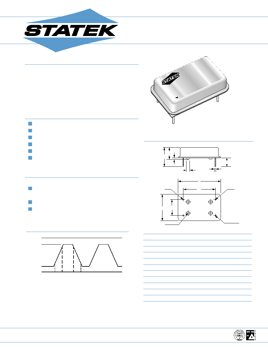
DESCRIPTION
The LXO-AT consists of a TTL and CMOS-compatible hybrid
circuit and a miniature quartz crystal packaged in a
hermetically-sealed metal DIP. Permanent, precision tuning
and a hermetically sealed AT quartz crystal allows for very tight
calibration tolerance and eliminates the need for a tuning
capacitor, a major source of long-term frequency drift.
FEATURES
Low aging
CMOS and TTL compatible
Double hermetically sealed package
Full military testing available
3 Volt model also available
Optional Tri-State or Output Enable
APPLICATIONS
Industrial, Computer & Communications
General purpose clock oscillator
Military
Flight recorder
Airborne hybrid computers
LXO-AT OSCILLATOR
500 kHz to 120 MHz
Low Power Crystal Oscillator
TM
V
DD
V
OH
t
r
t
f
0
V
OL
90%*
10%*
LX0-70.0MHz
* Of VDD
PACKAGE DIMENSIONS
B
C
PIN
NO.1
PIN
NO.14
PIN
NO.8
PIN
NO.7
G
F
E
H
D
A
J
I
DIM
INCHES
mm
A
0.810 MAX.
20.57 MAX.
B
0.510 MAX.
12.95 MAX.
C 0.300
0.005
7.62
0.13
D
0.600
0.005
15.24
0.13
E
0.430 TYP.
10.92 TYP.
F
0.240 MAX.
6.10 MAX.
G
0.040 TYP.
1.02 TYP.
H
0.150 MIN.
3.81 MIN.
I
0.018
0.002
0.46
0.05
J
0.070 TYP.
1.78 TYP.
* Position of bumps for reference only
+
_
+
_
+
_
+
_
+
_
+
_
OUTPUT WAVE FORM

STATEK CORPORATION 512 N. MAIN ST., ORANGE, CA 92868 714-639-7810 FAX: 714-997-1256 www.statek.com
10111 - Rev D
SPECIFICATIONS
Specifications are typical at 25oC unless otherwise noted.
Specifications are subject to change without notice.
Supply Voltage (V
DD
)
5V 10% (3.3V available)
Calibration
A:
0.01% (100ppm)
Tolerance (at 5V)*
B:
0.03%
C :
0.10%
Frequency
0
O
C to +50
O
C from
5 to
30ppm
Stability**
-10
O
C to +70
O
C from 10 to
50ppm
-40
O
C to +85
O
C from
20 to
100ppm
-55
O
C to +125
O
Cfrom 30 to 100ppm
Supply Current
4 mA to 60 mA (Depending on freq.)
Output Levels
V
OL
V
OH
TTL
0.4V MAX.
2.4V MIN.
CMOS
0.5V MAX.
4.5V MIN.
Start-up Time
5 msec. MAX.
Rise/Fall Time
6 nsec. Typ., 10 nsec. MAX.
Duty Cycle
40% Min., 60% MAX.
Aging, first year
10 ppm MAX.
Shock, survival***
1,000g peak 1 msec., 1/2 sine
Vibration survival
10g rms 10-2000 Hz
Operating Temperature -10
O
C to +70
O
C Commercial
-40
O
C to +85
O
C Industrial
-55
O
C to +125
O
C Military
Storage Temperature
-55
O
C to +125
O
C
* Tighter tolerances available for calibration and stability.
** Does not include calibration tolerance
*** High shock version available
Note: All parameters are measured at ambient temperature
with a 10M
and 10pF load at 5V
+
_
+
_
+
_
+
_
+
_
+
_
+
_
+
_
+
_
+
_
+
_
+
_
HOW TO ORDER LXO-AT CRYSTAL OSCILLATORS
LXO-AT
S
10
T
32 MHz
(
100ppm
/
100ppm
/
200ppm
/
I
)
"S" if special
2 = 2 LS TTL Load
E = Enable
Calibration
Frequency
Total Frequency
Temp. Range:
or custom
8 = 8 TTL Load
T = Tri-State
Tolerance*
Stability over
Tolerance
C = Commercial
design.
10 =10 TTL Load
N = Neither
@ 25
0
C
Temp. Range
I = Industrial
Blank if Std.
(A)
M = Military
(B)
S = Specify
(C)
* Other calibration fill in ppm
ABSOLUTE MAXIMUM RATINGS
Supply Voltage V
DD
-0.3V to 7V
Storage Temperature
-55
O
C to +125
O
C
TRUTH TABLE
PIN 1*
PIN 3
LXO-AT-8E
Low (0)
High (1)
High (1)
Freq. Output
LXO-AT-2E
Low (0)
Low (0)
High (1)
Freq. Output
LXO-AT-10T
Low (0)
High (Z)
High (1)
Freq. Output
* Normally high (internal pull-up resistor)
Frequency
___
ENABLE VS. TRI-STATE
Enable: When pin 1 is low (0), the oscillator stops
oscillation.
Tri-state: When pin 1 is low, the oscillator is running.
However, the output buffer amplifier stops
functioning and output is in high impedance
(Z) state.
Enable
Tri-state
Current consumption
when pin 1 is low
Low
High
Output recovery delay
when pin 1 changes from
Delayed
Immediate
low (0) to high (1)
PIN CONNECTIONS
1. Output Enable, INH (Tri-State) or NC
7. Ground
8. Output
14.
V
DD
PACKAGING
LXO-AT- Tube Pack (Standard)