 | –≠–ª–µ–∫—Ç—Ä–æ–Ω–Ω—ã–π –∫–æ–º–ø–æ–Ω–µ–Ω—Ç: STK6005 | –°–∫–∞—á–∞—Ç—å:  PDF PDF  ZIP ZIP |

1
STK6005
DATA SHEET
by
SYNTEK
Æ
=========STK6005=========
Flat Panel Scaler
Version 1.0
DESIGN CENTER
6F, YU FENG BLDG. 317 SUNG-CHANG RD., TAIPEI, TAIWAN, R.O.C.
TEL: 886-2-25056383
FAX: 886-2-25064323
HEADQUARTER
3F, NO.24-2, INDUSTRY E.RD., IV, SCIENCE-BASED INDUSTRIAL PARK, HSINCHU, TAIWAN, R.O.C.
TEL: 886-3-5773181
FAX: 886-3-5778010
©
©
©
C
C
Co
o
op
p
py
y
yr
r
ri
i
ig
g
gh
h
ht
t
t
S
S
SY
Y
YN
N
NT
T
TE
E
EK
K
KT
T
T
S
S
SE
E
EM
M
M I
I
IC
C
CO
O
ON
N
ND
D
DU
U
UC
C
CT
T
TO
O
OR
R
R
C
C
Co
o
or
r
rp
p
po
o
or
r
ra
a
at
t
ti
i
io
o
on
n
n
&
&
&
L
L
Li
i
ic
c
ce
e
en
n
ns
s
so
o
or
r
rs
s
s
(
(
(2
2
20
0
00
0
00
0
0)
)
).
.
.
A
A
Al
l
ll
l
l
r
r
ri
i
ig
g
gh
h
ht
t
ts
s
s
r
r
re
e
es
s
se
e
er
r
rv
v
ve
e
ed
d
d

2
STK6005
Caution!
The information in this document is subject to change without notice and does not
represent a commitment on part of the vendor, who assumes no liability or responsibility for
any errors that may appear in this data sheet.
No warranty or representation, either expressed or implied, is made with respect to the
quality, accuracy, or fitness for any particular part of this document. In no event DCNT the
manufacturer be liable for direct, indirect, special, incidental or consequential damages
arising from any defect or error in this data sheet or product. Product names appearing in
this data sheet are for identification purpose only, and trademarks and product names or
brand names appearing in this document are property of their respective owners.
This data sheet contains materials protected under International Copyright Laws. All
rights reserved. No part of this data sheet may be reproduced, transmitted, or transcribed
without the expressed written permission of the manufacturer and authors of this data sheet.

3
STK6005
STK60005 Data Sheet
Table of Contents
Item Page
1.
GENERAL DESCRIPTION
............................................................................................5
2.
FEATURES
........................................................................................................................5
2.1
General Features
.......................................................................................................5
2.2
Input
...........................................................................................................................5
2.3
Output
........................................................................................................................5
2.4
OSD Features
.............................................................................................................5
3.
BLOCK DIAGRAM
.........................................................................................................6
3.1
Application Diagram
.................................................................................................7
4.
PINS CONFIGURATION
................................................................................................7
4.1
ADC Interface
...........................................................................................................8
4.2
Panel Interface
...........................................................................................................8
4.3
OSD Interface
............................................................................................................8
4.4
Micro-Controller Interface
.......................................................................................8
4.5
Power Pins
..................................................................................................................9
4.6
Pin List
.......................................................................................................................9
5.
FUNCTION
.......................................................................................................................10
5.1
Input Timing and Format
........................................................................................10
5.2
Output Timing and Format
......................................................................................11
5.3
YUV to RGB Space Converter
.................................................................................12
5.4
De-Interlace
...............................................................................................................12
5.5
Input Synchronous signals Processing
....................................................................12
5.6
Definition of Input/Output Window
........................................................................13
5.7
Scaling Control
..........................................................................................................14
5.8
Operating Mode
........................................................................................................15
5.9
Contrast and Brightness Control
.............................................................................16
5.10
Gamma Correlation
................................................................................................16
5.11
Output Dithering
.....................................................................................................17
5.12
Clock System
...........................................................................................................17
5.13
OSD Control
............................................................................................................18
5.14
Auto-Adjustment
.....................................................................................................22
5.15
I2C Interface
............................................................................................................25
5.16
Interrupt
..................................................................................................................25
5.17
GPIO Ports
..............................................................................................................26

4
STK6005
6.
REGISTER DEFINITION
...............................................................................................26
6.1
ADC Control
..............................................................................................................26
6.2
Panel Window Control
..............................................................................................27
6.3
Scaling Control
..........................................................................................................27
6.4
Panel Output Control
...............................................................................................28
6.5
OSD Control
..............................................................................................................29
6.6
MISC Control
............................................................................................................30
6.7
Auto-Adjustment
.......................................................................................................30
6.7.1
Auto-Adjustment (1)
......................................................................................31
6.7.2
Auto-Adjustment (2)
......................................................................................33
7.
ELECTRICAL CHARACTERISTICS
..........................................................................33
7.1
Operating Conditions Recommended
.....................................................................33
7.2
DC Characteristics
....................................................................................................33
7.3
AC Characteristics
....................................................................................................34
8.
PACKAGE DIMENSION
................................................................................................35
9.
INFORMATION
...............................................................................................................36
9.1
Order Information
....................................................................................................36
9.2
Contact Information
.................................................................................................36

5
STK6005
1. GENERAL DESCRIPTION
The STK6005 chip, converting PC / Mac video images for a TFT-LCD display monitor, performs an image
scaler on the RGB / YUV image data stream and outputs the scaled pixels to the LCD panel. The chip embeds
line buffers for a scaling operation, so there is no external memory required. Both the OSD (On-Screen Display)
circuit and the interface are embedded in this chip to support the internal and external OSD. STK6005 also
provides an auto-adjustment function to automatically support the frequency & phase tuning, H / V positioning
and white balance tuning. A brightness and contrast control circuit and a Gamma table correction function are
also provided.
2. FEATURES
2.1 General Features:
. Single-chip video scaling solution, no external memory required
. Programmable independently horizontal and vertical scaling up and down
. Advanced filters provided to get a high quality scaling image
. Auto-adjustment to frequency, phase, H/V position, and white balance
. Hardware display mode and field detection
. Brightness and contrast control
. 10-bit Gamma table
. Dithering for 24-bit or 18-bit panel output
. Serial 2 wires of the I
2
C interface
. 0.25um CMOS technology with 3V I/O interface (5V tolerant input)
. 128 pins of the PQFP package
2.2 Input:
. Single pixel input port (24 bits) with input rates
up to 140MHz (SXGA @75Hz)
. DE input for digital interface
. Support to an 8-bit YUV 4:2:2 (CCIR-656) stream format and a 16-bit YUV 4:2:2 input
. Built-in YCbCr to RGB color space conversion circuit
. Support to a composite sync. separation and a coast / clamp control to ADC
2.3 Output:
. Dual pixel output ports (48 bits) with output rates up to 80MHz
. Maximum output resolution up to SXGA @ 85Hz
. Skew tuning between panel clock and output data
2.4 OSD features:
. On-chip internal OSD
Back to Contents Table

6
STK6005
. Support to a rotational OSD
. 128 fonts downloadable and 32 multi-color fonts maximum
. 256 OSD display characters
. Support to character transparent, blinking effects
. Color blending effect of OSD and video
. OSD ably zoomed to 2x independently for horizontal and vertical
. Shadow and border effect on OSD frame
. Support to an external OSD interface
3.
BLOCK DIAGRAM
Below shown is an
STK6005 internal block diagram:
STK6005
YUV to
RGB
R/G/B Input Pixels Scaling Line Scaling up
Sampling Down Buffers & Filtering
HS/VS H/V Sync Input Timing Timing Output Timing Brightness
Process Control Sync Control Contrast
PLL & Gamma
Clock Generator Correction
Dithering
Auto- Internal OSD
Adjustment Micro-Controller Output
Function Interface External OSD Mixer
SCL SDA R/G/B
Micro External LCD
Controller OSD Panel
Back to Contents Table

7
STK6005
3.1 Application Diagram
Shown below is an external application interface diagram:
4.
PINS CONFIGURATION
Back to Contents Table

8
STK6005
4.1 ADC Interface
Name
I/O
Description
Pin No.
Note
RIN[7:0]
I
Red input (RGB)
Y[7:0] input (YUV16)
YUV[7:0] input (YUV8)
111-104
GIN[7:0]
I
Green input (RGB) / UV[7:0] input (YUV16)
103-96
BIN[7:0]
I
Blue input (RGB) / YUV control input (YUV16)
Bit 7 : Href
Bit 6 : Vref
Bit 5 : Hsync
Bit 4 : Vsync
Bit 3 : Field
Bit 2 : LLC2
Bit 1 : Cref
95-88
VCLK
I
Video input clock / YUV LLC clock
114
HSI
I
RGB horizontal sync input (after ADC)
115
CSync
I
Composite sync input (from SOG)
116
VSI
I
RGB vertical sync input
117
VGAHS
I
Original VGA H-Sync input (before ADC)
118
ExtDE
I
External DE input
119
Clamp
O
Clamp signal to ADC
120
RGHS
O
To regenerate an H-Sync output
121
MaskVS
O
Coast signal to ADC
122
4.2 Panel Interface
Name
I/O
Description
Pin No.
Note
PE_R[7:0]
O
Even port (port A) red output
60-57, 54-51
PE_G[7:0]
O
Even port (port A) green output
50-45, 40-39
PE_B[7:0]
O
Even port (port A) blue output
38-31
PO_R[7:0]
O
Odd port (port B) red output
24-17
PO_G[7:0]
O
Odd port (port B) green output
16-15, 10-5
PO_B[7:0]
O
Odd port (port B) blue output
4-1, 126-123
DCLK
O
Panel data clock output
29
PHS
O
Panel H-Sync output
25
PVS
O
Panel V-Sync output
26
PDE
O
Panel data enable output
27
ExtPCLK
I
External panel clock input
69
4.3 OSD Interface
Name
I/O
Description
Pin No.
Note
OVVS
O
Overlay V-Sync output
74
OVHS
O
Overlay H-Sync output
75
OVCLK
O
Overlay clock output
76
OVR
I
Overlay red input
77
OVG
I
Overlay green input
78
OVB
I
Overlay blue input
79
OVI
I
Overlay intensity input
80
OVFB
I
Overlay color enable
81
4.4 Micro-Controller Interface
Name
I/O
Description
Pin No.
Note
SDA
I/O I
2
C bus data
82
Back to Contents Table

9
STK6005
SCL
I
I
2
C bus clock
83
INTN
O
Interrupt request output (active low)
84
RSTN
I
Device reset input (active low)
85
RefCLKI
I
Crystal oscillator input
70
RefCLKO
O
Crystal oscillator output
71
GPIO3-0
I/O General purpose I/O and PWM
64-61
4.5 Power Pins
Name
P/G
Description
Pin No.
Note
VDD2
P
Digital power supply for core cells
12,42,87,113
2.5V
VSS2
G Digital ground for core cells
11,41,86,112
0V
VDD3
P
Digital power supply for I/O cells
14,30,44,56,73, 128
3.3V
VSS3
G Digital ground for I/O cells
13,28,43,55,72, 127
0V
VDD2P
P
Digital power supply for PLL
68
2.5V
VSS2P
G Digital ground for PLL
67
0V
AVDD
P
Analog power supply for PLL
66
2.5V
AVSS
G Analog ground for PLL
65
0V
4.6 Pin List
Pin No.
Pin Name
Pin No.
Pin Name
Pin No.
Pin Name
Pin No.
Pin Name
1
PO_B[4]
33
PE_B[2]
65
AVSS
97
GIN[1] / UV[1]
2
PO_B[5]
34
PE_B[3]
66
AVDD
98
GIN[2] / UV[2]
3
PO_B[6]
35
PE_B[4]
67
VSS2P
99
GIN[3] / UV[3]
4
PO_B[7]
36
PE_B[5]
68
VDD2P
100
GIN[4] / UV[4]
5
PO_G[0]
37
PE_B[6]
69
ExtPCLK
101
GIN[5] / UV[5]
6
PO_G[1]
38
PE_B[7]
70
RefCLKI
102
GIN[6] / UV[6]
7
PO_G[2]
39
PE_G[0]
71
RefCLKO
103
GIN[7] / UV[7]
8
PO_G[3]
40
PE_G[1]
72
VSS3
104
RIN[0] / Y[0]
9
PO_G[4]
41
VSS2
73
VDD3
105
RIN[1] / Y[1]
10
PO_G[5]
42
VDD2
74
OVVS
106
RIN[2] / Y[2]
11
VSS2
43
VSS3
75
OVHS
107
RIN[3] / Y[3]
12
VDD2
44
VDD3
76
OVCLK
108
RIN[4] / Y[4]
13
VSS3
45
PE_G[2]
77
OVR
109
RIN[5] / Y[5]
14
VDD3
46
PE_G[3]
78
OVG
110
RIN[6] / Y[6]
15
PO_G[6]
47
PE_G[4]
79
OVB
111
RIN[7] / Y[7]
16
PO_G[7]
48
PE_G[5]
80
OVI
112
VSS2
17
PO_R[0]
49
PE_G[6]
81
OVFB
113
VDD2
18
PO_R[1]
50
PE_G[7]
82
SDA
114
VCLK
19
PO_R[2]
51
PE_R[0]
83
SCL
115
HSI
20
PO_R[3]
52
PE_R[1]
84
INTN
116
CSync
21
PO_R[4]
53
PE_R[2]
85
RSTN
117
VSI
22
PO_R[5]
54
PE_R[3]
86
VSS2
118
VGAHS
23
PO_R[6]
55
VSS3
87
VDD2
119
ExtDE
24
PO_R[7]
56
VDD3
88
BIN[0]
120
Clamp
25
PHS
57
PE_R[4]
89
BIN[1] / Cref
121
RGHS
26
PVS
58
PE_R[5]
90
BIN[2] / LLC2
122
MaskVS
27
PDE
59
PE_R[6]
91
BIN[3] / Field
123
PO_B[0]
28
VSS3
60
PE_R[7]
92
BIN[4] / Vsync
124
PO_B[1]
29
DCLK
61
GPIO0
93
BIN[5] / Hsync
125
PO_B[2]
30
VDD3
62
GPIO1
94
BIN[6] / Vref
126
PO_B[3]
31
PE_B[0]
63
GPIO2
95
BIN[7] / Href
127
VSS3
32
PE_B[1]
64
GPIO3
96
GIN[0] / UV[0]
128
VDD3
Back to Contents Table

10
STK6005
5. FUNCTION
5.1 Input Timing and Format
This chip supports a 24-bit RGB input (up to SXGA 75Hz) of a single port, a 16-bit YUV 4:2:2 input,
and an 8-bit YUV 4:2:2 (CCIR-656) video input. The timing diagrams are provided below.
For RGB input format, the RGB data (RIN/GIN/BIN ports) and H-Sync (HSI), V-Sync (VSI) are
sampled at the rising or falling edge of VCLK.
For TMDS input format, a control signal ExtDE can be provided to define the valid data.
For video input format, the input YUV ports are shared with RIN/GIN/BIN ports. The 16-bit YUV 4:2:2
format uses RIN[7:0] for Y[7:0], GIN[7:0] for UV[7:0], and BIN[7:1] for YUV control bus. Hsync / Vsync
are used as H-Sync and V-Sync input signals. Cref is used as a clock edge qualifier. Href and Vref are
used to define the valid data. Field input is used as the odd / even fields indicator.
The 8-bit YUV 4:2:2 (CCIR-656) format uses RIN[7:0] for data input YUV[7:0], and the timing control is
also embedded in the data stream. Therefore, there are no control signal connections needed for this
format.
VCLK
R/G/BIN RGB0 RGB1 RGB2
HSI/VSI
ExtDE
RGB input format timing diagram
Back to Contents Table

11
STK6005
5.2 Output Timing and Format
The output interface consists of two pixel ports, each containing Red / Green / Blue in colors with 6 or 8
bits of resolution. There are three output control signals for panel ≠ PVS, PHS and PDE. The output
pixels and control signals above are all synchronous to the active edge of panel output clock DCLK. The
polarity of output clock / control signals and the timing of the active edge of output clock are
programmable by setting the internal registers.
There are two output formats ≠ single / dual pixels output modes. In single pixel output mode, pixel data
are output from PE_R/G/B ports only, and the PO_R/G/B ports are disabled. In dual pixel output mode,
pixel data are output to both PE_R/G/B and PO_R/G/B ports in parallel. The first pixel of a line will be
output to PE_R/G/B ports and the second pixel will be output to PO_R/G/B ports.
Back to Contents Table
VCLK
Cref
Y(RIN) Y0 Y1 Y2
UV(GIN) U0 V0 U2
Hsync/Vsync
/Field
Href/Vref
YUV16 input format timing diagram

12
STK6005
5.3 YUV to RGB Space Converter
For video input (EnYUV = 1), the input YUV (YCbCr) data are converted internally into RGB format by
the following equations.
R = Y + 1.371 (Cr ≠ 128)
G = Y - 0.698 (Cr ≠ 128) ≠ 0.336 (Cb ≠ 128)
B = Y + 1.732 (Cb ≠ 128)
5.4 De-Interlace
For interlace input, the input image is separated into even and odd fields. Due to no frame buffer
available, STK6005 employs the spatial interpolation method to calculate the missing lines from their
neighboring lines. Internal register 0x1C should be set to enable a de-interlace function.
5.5 Input Synchronous Signals Processing
STK6005 provides a composite sync separation hardware to separate V-Sync from C-Sync and re-
generate the H-Sync for the external ADC chip. STK6005 supports three combinations of input H / V
synchronous signals (before ADC) which are composite sync signal from CSync or from VGAHS port, and
separated sync signals from the VGAHS and VSync ports. An H-Sync output will be re-generated from
DCLK
PE_R/G/B RGB0 RGB1 RGB2 RGB3 RGB4 RGB5 RGB6 RGB7
PO_R/G/B Hi-Z / 0
PVS/PHS
PDE
Single port output mode timing diagram
DCLK
PE_R/G/B RGB0 RGB2 RGB4 RGB6 RGB8
PO_R/G/B RGB1 RGB3 RGB5 RGB7 RGB9
PVS/PHS
PDE
Dual port output mode timing diagram
Back to Contents Table

13
STK6005
the VGAHS or CSync signals for the external ADC H-Sync input. And suitable coast and clamp signals are
also generated for external ADC.
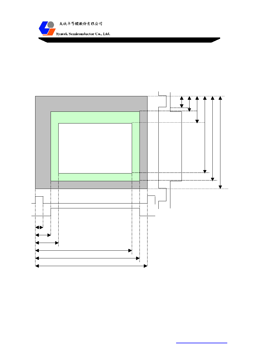
5.6 Definition of Input / Output Window
The input capture window is defined by the internal registers: HBP, HDISP, VBP, and VDISP (if SelDE
is set to 0). The timing of inputs are referred to the leading edge of input H-Sync and V-Sync. The
horizontal timing is counted in the number of VCLKs and the vertical timing exists in input display lines.
VBP
VDISP
Input Sampling Area
IVT
HBP HDISP
IHT
Input window diagram
Back to Contents Table
14
STK6005
The panel output window are defined by the following registers: PHSW, PHDE1, PHDE2, PHXDE1,
PHXDE2, PHT, PVSW, PVDE1, PVDE2, PVXDE1, PVXDE2, PVT. The output timing are referenced to
the leading edge of PHS and PVS. The horizontal timing is counted by number of output pixels and the
vertical timing is in output display lines.
Output window definition diagram
5.7 Scaling Control
The input image can be independently scaling up and down in both horizontal and vertical directions.
The scaling ratio for each direction is in the range of 0.5x ~ 16x. The registers HSR and VSR control the
output scaling ratio for horizontal and vertical directions respectively. The formula to calculate the values
of HSR and VSR are shown below:
P
V
T
P
V
D
E
2
PVXDE2
PVXDE1
P
V
D
E
1
P
V
S
W
P
V
D
E
P
V
S
Blanking
Panel
Input Image Display Area
PHS
PDE
PHSW
PHDE1
PHXDE1
PHXDE2
PHDE2
PHT
Back to Contents Table

15
STK6005
HSR = horizontal input display resolution / output display resolution * 32768
VSR = vertical input display resolution / output display resolution * 32768
This chip provides 6 advanced filters to get a high quality-scaling image for requirements on different
sharpness. Set EnFilt flag to 1 to enable scaling function using the filter defined by FiltType register.
5.8 Operating Mode
STK6005 uses internal line buffers to perform the scaling function. Since there is no external frame buffer
serving as a frame rate converter, the output vertical frequency is always equal to the input vertical frequency
during normal operation. The period of PCLK should be programmed as close as the formula listed below to
avoid over-run / under-run conditions of internal line-buffers.
Period of PCLK = Period of VCLK * RateH * RateV
where
RateH = total pixels of an input line / total pixels of an output line
RateV = total input lines / total output lines
= total input display lines / total output display lines
STK6005 provides three operating modes to synchronize the input and output display timing:
1. Free-run mode:
EnSyncH {0x3D[7]} = 0
EnSyncV {0x3D[6]} = 0
In this mode, there is no timing relationship between the input and output timing. Registers PHT and
PVT control the output horizontal period and vertical period respectively. For this mode, even if no input
signal comes, the output timing can also be generated automatically. This mode is used when there is no
valid input or used for testing purpose.
2. Synchronization to Input V-Sync:
EnSyncH {0x3D[7]} = 0
EnSyncV {0x3D[6]} = 1
In this mode, the input vertical timing has impacted on the output vertical timing. The input V-Sync
leading edge will generate a locking event to lock the output display timing. Therefore, the output vertical
period will keep the same as the input vertical period. The latency between the input V-Sync leading edge
and the locking event can be programmed through registers DlyLine and DlyPxl. The output horizontal
period is set by PHT. The PVT value should be set to maximum (0x7FF) value for this mode. For the
advantage of this mode, all output horizontal periods are equal. For the disadvantage of this mode, when
some errors occur in the real output video clock (PCLK) and in the ideal output video clock (VCLK *
RateH * RateV), the buffer overrun or underrun may happen internally due to the accumulation of errors.
Back to Contents Table

16
STK6005
3. Synchronization to Input V-Sync and H-Sync:
EnSyncH {0x3D[7]} = 1
EnSyncV {0x3D[6]} = x
In this mode, the input timing also has impacted on the output horizontal and vertical timings. The
input V-Sync leading edge will also generate a lock event to lock the output display timing. Therefore, the
output vertical period will keep the same as the input vertical period. But the output horizontal period is
gained by (EmPHT / 16) cycles of input VCLK to keep output horizontal timing tracking to input
horizontal timing. The register EmPHT should be set to the value of input horizontal period (in pixels) *
RateV * 16, where the RateV = total input lines / total output lines. The register value of PHT will be
ignored. The register value of PVT should be set to maximum (0x7FF) value for this mode. For the
advantage of this mode, even when some errors result in the real output video clock (PCLK) and in the
ideal output video clock (VCLK * RateH * RateV), the buffer overrun or underrun will not happen
internally due to the accumulation of errors. For the disadvantage of this mode, each output horizontal
period may be somewhat different.
5.9 Contrast and Brightness Control
STK6005 can adjust the contrast and brightness of output pixels after scaling operation. Registers GainR,
GainG, and GainB adjust the contrast of red, green, and blue respectively for output pixels. Registers
DC_R, DC_G, DC_B adjust the brightness for output pixels. Gain registers are those with an 8-bit
unsigned value and DC registers are those in a 2's complement format. The adjustment formula is listed
below:
Red (out) = Red(in) * GainR / 128 + DC_R
Green (out) = Green(in) * GainG / 128 + DC_G
Blue (out) = Blue(in) * GainB / 128 + DC_B
5.10 Gamma Correlation
STK6005 provides an 8-to-10 bits of the color look-up table for each color channel intended for Gamma
correction. A 10-bit output results in an improved color depth control. The 10-bit output is then
dithered down to 8 or 6 bits per color for display output. The Gamma look-up table (LUT) is user-
programmable to provide an arbitrary transfer function.
Before the Gamma LUT is programmed, the Gamma correction function should be disabled first and
then decides which Gamma LUTs of colors is to be programmed. The Gamma LUT will be written at the
same time if the GmaWE flag for respective color is set to 1. The programming steps are shown as below:
1. Disable Gamma correction function (set EnGamma flag to 0).
2. Set respective GmaWE flag of each color to 1 to enable programming.
3. Write start programming address into uWrGmaA register.
Back to Contents Table
17
STK6005
4. Write lower 8 bits, and then write higher 2 bits data into uWrGmaD register to program
a 10-bit Gamma value.
5. Go to step 4 for continuing to write the next address.
Go to step 3 for changing another address.
Go to step 2 for changing another Gamma LUT.
Go to next step to stop Gamma LUT programming.
6. Enable Gamma correlation function (set EnGamma flag to 1).
5.11 Output Dithering
The Gamma LUT outputs a 10-bit value for each color channel. This value can be dithered down to
either 8 bits for 24 bits per pixel panels, or 6-bit for 18 bits per pixel panels. Dithering works by spreading
the quantization error over neighboring pixels both spatially and temporarily. The dithering benefits and
improves the effective color depth because the humans' eyes will tend to average neighboring pixels and a
smooth image free of contours will be perceived.
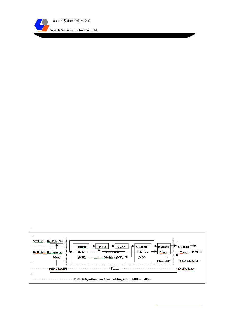
5.12 Clock System
STK6005 takes input clock (VCLK) from external ADC or video decoder chips. The input pixels are
latched on the rising edge of VCLK by default. The input phase of VCLK can be inverted by setting
SetICLK flag to 1.
The internal panel clock PCLK can be obtained either from an external source (from ExtPCLK pin) or
generated from an internal PLL. The PLL takes the external crystal oscillator input (14.3MHz) or VCLK
as clock source to synthesize the clock for panel. The clock frequency synthesized by PLL can be
programmed to support different display modes. The panel clock is output to DCLK with equal or 1/2 of
frequency of PCLK for single or dual pixel output modes respectively. The output delay and phase of
DCLK can be programmed by internal registers SetDCLK and DlyDCLK. The PLL block diagram and
control registers are depicted as follows:
Back to Contents Table

18
STK6005
Notes:
1.
The frequency derived from PLL frequency synthesizer is formulated as follows:
Fout (PCLK) = Fin * NF / (NR * NO).
Where
NF = PLL_M[8:0] + 2
NR = PLL_N[4:0] + 2
NO = 1 / 2 / 2 / 4 when PLL_OD[1:0] = 00 / 01 / 10 / 11
2.
Meanwhile, the following constraints must be followed:
Fref = Fin / (NR * 2)
The comparison frequency (Fref) should be in the range of 800KHz to 8MHz.
Fvco = Fin * NF / NR
The output frequency of VCO should be in the range of 100MHz to 200MHz.
5.13 OSD Control
Display Area of OSD
The following diagram shows the display area definition of STK6005 OSD.
Register Width and Length of the unit is in characters; others are in lines or pixels. The values of
registers StartV and StartH are calculated from the synchronous point of panel output.
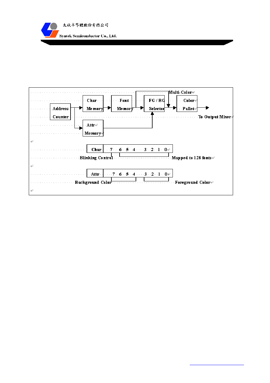
Architecture of the OSD (On-Screen Display)
STK6005 provides up to 256 sets of characters and attributes to display the OSD contents. Provided is
that 128 internal soft fonts (12 * 18 dots) can be selected to display for each character. The 8-bit attribute of
each character consists of the foreground color and background color indices mapped to 16 colors of the
pallet. The background transparent effect will be enabled when the background color index is set to 0xF.
Back to Contents Table
19
STK6005
A blinking effect will appear in the character if a bit 7 Char index is set to 1. The foreground and
background color is mapped to one of 16 sets of the color pallet. Each set of color pallet is in 24 bits of
true color. The following diagram shows the architecture of STK6005 OSD.
To Set a Character and an Attribute
For a char displayed on location (X, Y) of OSD window, the converting formula of the Char / Attribute
memory address is shown as follows:
Memory Address = Y * Width + X
X indicates the horizontal position of the Char in OSD window (in unit of Char)
Y indicates the vertical position of the Char in OSD window (in unit of Char)
Width explains the horizontal duration of OSD window (in unit of Char)
Two sequences can be applied to write the Char / Attribute contents:
You can write Char / Attribute separately by setting CharOnly = 1. The memory address will
automatically increase 1 after you write a Char or an Attribute, and then you can write a next Char or an
Attribute content. Or you can write Char / Attribute pairs by setting CharOnly = 0. The memory
address will not automatically increase 1 until an Attribute is written in. The steps to set Char and
Attribute are shown as follows:
1. Calculate and set a memory address (write uWrAdr).
2. Write a Char index (write uWrChr). If CharOnly = 1, go to step 4.
3. Write an Attribute index (write uWrAttr).
4. Go to step 2 for continuing to set a next position of Char.
Go to step 1 to recalculate a new address or stop the procedure.
Back to Contents Table
20
STK6005
To
Set a Color Pallet
STK6005 provides 16 sets of color pallets. Each set of color pallet is provided with 24 bits and can be set
to any color. The attributes of OSD char are indexes for foreground and background colors and mapped
to 24-bit colors by this color pallet. The steps to set the color pallet are shown as follows:
1. Set a color pallet No. (write uWrAdr)
2. Set a red color in the current color pallet. (write uWrColor)
3. Set a green color in the current color pallet. (write uWrColor)
4. Set a blue color in the current color pallet. (write uWrColor)
5. Go to step 2 for continuing to set a next color pallet.
Go to step 1 to set another color pallet No. or stop the procedure.
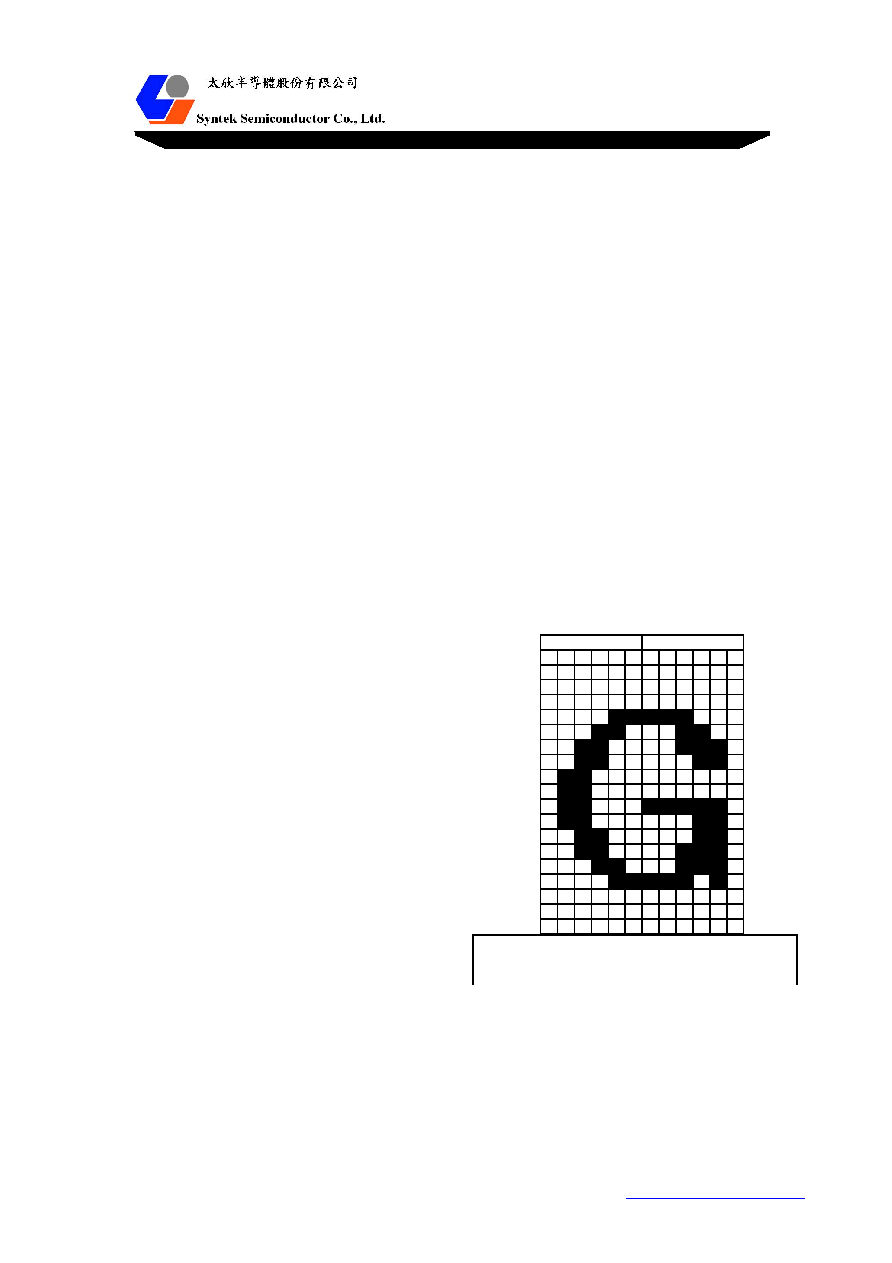
Architecture of OSD Fonts
STK6005 provides 128 sets of 12*18 fonts downloadable.
Each font can be programmed by writing 36 * 6-bit bit-map data.
The bit-map data sequences are shown in the following example:
Font writing sequence
1. Set a font No. (write uWrAdr).
2. Write 36 bytes of bit-map data.
(each data consists of 6 pixels) into the font
memory sequentially (write uWrFont).
3. Go to step 2 for continuing to write a
next font.
Go to step 1 for setting another font No.
Or stop the procedure.
Byte0
Byte1
5
0 5
0
ROW-00
0x00
ROW-01
0x02
ROW-02
0x04
ROW-03
0x06
ROW-04
0x08
ROW-05
0x0A
ROW-06
0x0C
ROW-07
0x0E
ROW-08
0x10
ROW-09
0x12
ROW-10
0x14
ROW-11
0x16
ROW-12
0x18
ROW-13
0x1A
ROW-14
0x1C
ROW-15
0x1E
ROW-16
0x20
ROW-17
0x22
Font "G" example
Back to Contents Table

21
STK6005
To set a Multi-Color Font
Set a register MultiChar to capture the color fonts. Each color font will occupy 4 monochrome fonts spaces.
The multi-color font will occupy the space from the font index 0. For example, when MultiChar is set to 2, there
are 2 multi-color fonts available. The monochrome fonts will start from font No. 8. The font No. 0 to 3 are
mapped to the same color font and the font NO. 4 to 7, the other color font. The color for each pixel of a color
font is also mapped to a 24-bit color through the color pallet as below.
To
set an OSD Double Size
To set registers DPH / DPV = 1 will stretch the OSD by a factor of two in the horizontal / vertical
direction respectively. Pixel and line replication is used to stretch the image. This option will also affect
the border and shadow size around the OSD window.
Blending Effect
STK6005 provides an effect of the blending OSD with image pixel and this effect is suitable for OSD
fade-in / fade-out effect. 16 levels of blending are supported. Blend level (defined by a register BlendR)
for binary codes "1111" through "0000" are in the proportion of 6.25%, 12.5%, 18.75%, .. , 93.75% and
100%. The blend percentage levels depicted here are in the percentage of OSD pixel data. For example,
0001 yields an output data stream whose blended pixel data contains 93.75% OSD and 6.25% underlying
image data. This OSD would be only slightly translucent.
External OSD interface
STK6005 also provides an external OSD interface to use an external OSD chip. OVCLK, OVHS,
OVVS ports will output the timing of panel clock, H-Sync, and V-Sync to the external OSD chip. The
output delay between OVCLK and OVHS / OVVS is tunable through register DlyOVCLK and DlyOVHS.
OSD pixels data are input from OVI, OVB, OVG, and OVR and will be combined into a 4-bit color index
then mapped to the color pallet. OVFB indicates the pixels to be displayed on the panel.
Rotational OSD
STK6005 also provides an internal logic to support the rotational OSD. When a font table for
Bit0
Bit1
Bit2 Combine to a 4-bit color font
Font 4N Bit3 Map to Color Pallet
Font 4N+1
Font 4N+2
Font 4N+3
Back to Contents Table

22
STK6005
rotational OSD is defined, the bit map of fonts should rotate by 90 degrees and be programmed for each
font of 36 bytes by 18 dots (3 bytes) * 12 lines. The char. and attribute contents of the OSD window
should also be programmed from bottom at a corner to the left first. (from bottom to top and then from left
to right) It should be noted that the registers for defining the OSD window are swapped between the
horizontal and vertical.
5.14 Auto-Adjustment
To set a Color Threshold
Set the threshold of input signals before using the auto-detecting function to avoid the noise of input signals
affecting the measurement results. Registers GateR, GateG, and GateB mean the threshold values for red,
green, and blue of input signals. The auto-detecting circuit will allow the input signals with all colors
levels higher than their thresholds level, or otherwise the input signals will not be included in the
measurement.
To
set a Measurement Window
Set the measurement window before using the auto-detecting function to avoid the noise of input signals among
some certain positions or to measure the region of interests. Set register SelWDE to switch the active region
defined by AWinH/V registers or internal DE.
To select an Input Source
Set a register SelHV to select H-Sync and V-Sync input sources for timing measurement. Set registers
SelVCnt and SelHCnt to select horizontal and vertical clocks for timing measurement.
Source Timing Measurement
STK6005 provides the following source timing data for auto-adjustment
1. HCT: A 16-bit value indicates the 16-cycle period of selected input H-Sync signal.
The selected input clock RefCLK or VCLK is used to measure the period.
This value will be updated in each frame.
2. VCT: A 12-bit value indicates the period of selected input V-Sync signal.
The period can be measured by the input horizontal line or by 144 * RefCLKs.
This value will be updated in each frame.
Video 1
Level
Threshold
0
Back to Contents Table

23
STK6005
3. VSHC: A 12-bit value indicates the horizontal position (counted from H-Sync leading
edge) of the selected input V-Sync leading edge. This value can be used as a field
indicator for interlace input signal to determine whether the incoming field is even or odd.
This value will be updated in each frame.
4. HPOSL: The 12-bit value indicates the left position of input image. VCLK is the
reference clock. This value will be updated in each frame.
5. HPOSR: The 12-bit value indicates the right position of input image. VCLK is the
reference clock. This value will be updated in each frame.
6. VPOST: The 11-bit value indicates the top position of input image. This value is
counted by input horizontal lines and updated in each frame.
7. VPOSB: The 11-bit value indicates the bottom position of input image. This value is
counted by input horizontal lines and updated in each frame.
8. HSLost: This flag is set to 1 when the input H-Sync period overflows.
9. VSLost: This flag is set to 1 when the input V-Sync period overflows.
10. HSPol: This flag determines whether the polarity of selected input H-Sync is positive (0) or
negative (1).
11. VSPol: This flag determines whether the polarity of selected input V-Sync is positive (0) or
negative (1).
Back to Contents Table

24
STK6005
Source Level Measurement
The auto-detecting circuit can detect the minimum and maximum values (MinR, MinG, MinB, MaxR,
MaxG, and MaxB) of the input video data for the contrast adjustment of external ADC. The
measurement window also defines the measurement region of input image.
Source Clock Phase Measurement
STK6005 provides two methods to adjust the sampling phase for external ADC. The first method detects
the toggles of input image (above or below the threshold). The auto-detecting circuit can find the position
with maximum toggle rate and then reveals its position (TGX, TGY) and its toggle rate (TogRate). With
this information, you can set the capture position (SetX, SetY) to capture the toggle data of 16 adjoining
pixels. The 16 toggle data (LVD) will be captured in each frame and a block of this chip automatically
compares said data (LVD) with the results of previous frame. The comparison results will be put in
register EQC to show how many toggle data are equal to those of previous frame.
The other method is to sum up the pixel values and difference (absolute value) between adjacent pixels of
input video. The measurement window defines the image region for calculation. The colors for
calculation can be selected by MaskRGB flags (1 = enable calculating). Some LSBs of summing data can
be truncated to avoid the noise of input video by setting the register MaskBit. The total sum of pixels'
difference can be used as a merit to adjust the external ADC to correct the phase and frequency.
VPOST
Input Image
VPOSB
VCT
HPOSL
HPOSR
HCT
H-Sync
VHSC
V-Sync
Back to Contents Table

25
STK6005
Buffer Status Detection
STK6005 detects the operation of internal buffer and provides the information to correctly synchronize the input
and output image. The registers of buffer status are shown below:
1. OverRun: This flag is set to 1 when the input rate of input image is larger than the output rate. Some input
video data are overwritten before output.
2. UnderRun: This flag is set to 1 when the output rate of output image is larger than the input rate. Some
input video data are not available for output.
3. BufUsage: This 16-bit value indicates the maximum buffer usage. A bit 15 is also an indicator for underrun.
Bits 14 to 11 indicate the maximum line usage of internal buffer. Bits 10 to 0 indicate the pixel
usage of internal buffer.
4. PosVXDE: This 11-bit value indicates the vertical position (lines) of input image stored in the internal
buffer when STK6005 starts to output the first video data of a frame. This value should be
in range of 3 ≠ 5 for a correct input-output synchronization.
5. PosHXDE: This 11-bit value indicates the horizontal position (pixels) of input image stored in internal
buffer when STK6005 starts to output the first video data of a frame.
5.15 I
2
C Interface
STK6005 supports the industrial 2-wire serial bus interface to communicate with external micro-controller.
The interface consists of an input pin SCL for serial clock and a bi-directional pin SDA for input / output
data. The slave address of this chip is 1111010x (F4H for write and F5H for read operations). The I2C
block will auto-increase the register address after each data write-in or read-out. For the operation timing
and protocol, please refer to the 2-wire serial bus specification.
5.16 Interrupt
STK6005 provides 8 interrupt flags to tell the micro-controller when the defined internal events happen.
The INTN pin will output low when any interrupt flag is being set. The interrupt flag register indicates
what events trigger the interrupt. To write data to the interrupt enable register (0x7F) will automatically
Video P5
Level
P1 P2 P3 P4 P5
Back to Contents Table

26
STK6005
clear the interrupt flags and reset INTN output to high.
5.17 GPIO Ports
STK6005 provides four general purpose inputs / outputs. These provide additional
signals to control the various devices in the system. Each GPIO port can be
independently programmed to input or output a direction (SelGPO) or a pulse width
modulation output (SelPWM).
6. REGISTER DEFINITION
6.1 ADC Control
Address
Bit
Name
Initial R/W
Description
0x10
[7:0]
HBP[7:0]
0x28
R/W
0x11
[3:0]
HBP[11:8]
0x1
R/W
Horizontal back-porch length of input video, unit in
number of input clocks
0x12
[7:0]
HDISP[7:0]
0x00
R/W
0x13
[3:0]
HDISP[11:8]
0x4
R/W
Horizontal display active length of input video, unit in
number of input clocks
0x14
[7:0]
VBP[7:0]
0x23
R/W
0x15
[2:0]
VBP[10:8]
0x0
R/W
Vertical back-porch length of input video, unit in number
of input scan lines
0x16
[7:0]
VDISP[7:0]
0x00
R/W
0x17
[2:0]
VDISP[10:8]
0x3
R/W
Vertical display active length of input video, unit in
number of input scan lines
0x18
[7:5]
ClampSTA
0x2
R/W Clamp start from RGHS trailing edge ( # of RefCLKs)
[4:0]
ClampPW
0x08
R/W Clamp output pulse width ( # of RefCLKs)
0x19
[7:4]
MaskBW
0x4
R/W Backward expansion width of VS mask (# of lines)
[3:0]
MaskFW
0x4
R/W Forward expansion width of VS mask (# of lines)
0x1A
[5]
EnClamp
0
R/W 0/1 : Clamp output low / enable
[4]
SetClamp
0
0/1 : to set Clamp output polarity to positive / negative
[3]
MaskSync
1
0/1 : MaskVS sync to RGHS leading / trailing edge
[2]
MaskExp
1
1 : enable MaskVS expansion
[1]
EnMaskVS
0
0/1 : MaskVS output low / enable
[0]
SetMask
0
0/1 : to set MaskVS output polarity to positive / negative
0x1B
[6]
SetICLK
0
R/W 0/1 : to set input clock polarity to positive / negative
[5]
SetIVS
0
0/1 : to set input Vsync polarity to positive / negative
[4]
SetIHS
0
0/1 : to set input Hsync polarity to positive / negative
[3]
HVMode
0
1 : VGAHS is composite sync and separates VS from it.
[2]
SelCSync
0
1 : to select Csync as Hsync / Vsync input
[1]
EnRGHS
1
0/1 : RGHS output low / enable
[0]
SetRGHS
0
0/1 : to set RGHS output polarity to positive / negative
0x1C
[5]
EnInter
0
R/W 1 : to enable a de-interlace function
[4]
L1Odd
1
1 : to indicate that Odd field is a first frame
[3]
HalfOdd
0
1 : VS active at half of HS period is an Odd field.
[2]
AdjEvenF
0
1 : to delay an active area of even field by 1 line
[1]
AdjOddF
0
1 : to delay an active area of odd field by 1 line
[0]
SelIntF
0
0/1 : YUV field is indicated by Field / HV sync timing.
Back to Contents Table

27
STK6005
0x1D
[7]
SelDE
0
R/W 0/1 : to select register setting / ExtDE as display active
[6]
EnYUV
0
1 : to select a YUV input
[5]
SetVref
0
0/1 : to set Vref polarity to positive / negative
[4]
SetHref
0
0/1 : to set Href polarity to positive / negative
[3]
SetCref
0
0/1 : to set Cref polarity to positive / negative
[2]
SetField
0
0/1 : to set Field (Odd) polarity to positive / negative
[1]
YUV16
0
0/1 : video format is a 8-bit (CCIR 656) / 16-bit format.
[0]
SelLLC2
0
1 : to select LLC2 as input clock
0x1E
[7:0]
VSDelay
0x04
R/W Delay of internal Vsync (* 8 input clocks)
6.2 Panel Window Control
Address
Bit
Name
Initial R/W
Description
0x20
[7:0]
PHDE1[7:0]
0x28
R/W
0x21
[3:0]
PHDE1[11:8]
0x1
R/W
Panel horizontal DE start position (# of PCLKs)
0x22
[7:0]
PHDE2[7:0]
0x28
R/W
0x23
[3:0]
PHDE2[11:8]
0x5
R/W
Panel horizontal DE end position (# of PCLKs)
0x24
[7:0]
PHXDE1[7:0]
0x28
R/W
0x25
[3:0]
PHXDE1[11:8]
0x1
R/W
Panel horizontal image start position (# of PCLKs)
0x26
[7:0]
PHXDE2[7:0]
0x28
R/W
0x27
[3:0]
PHXDE2[11:8]
0x5
R/W
Panel horizontal image end position (# of PCLKs)
0x28
[7:0]
PHT[7:0]
0x40
R/W
0x29
[3:0]
PHT[11:8]
0x5
R/W
Panel horizontal total (# of PCLKs)
set PHT = 0xFFF if EnSyncH = 1
0x2A
[7:0]
PHSW[7:0]
0x88
R/W Panel horizontal sync width (# of PCLKs)
0x2B
[7:0]
PVSW[7:0]
0x06
R/W Panel vertical sync width (# of lines)
0x2C
[7:0]
PVDE1[7:0]
0x23
R/W Panel vertical DE start position (# of lines)
0x2D
[2:0]
PVDE1[10:8]
0x0
R/W
0x2E
[7:0]
PVDE2[7:0]
0x23
R/W Panel vertical DE end position (# of lines)
0x2F
[2:0]
PVDE2[10:8]
0x3
R/W
0x30
[7:0]
PVXDE1[7:0]
0x23
R/W Panel vertical image start position (# of lines)
0x31
[2:0]
PVXDE1[10:8]
0x0
R/W
0x32
[7:0]
PVXDE2[7:0]
0x23
R/W Panel vertical image end position (# of lines)
0x33
[2:0]
PVXDE2[10:8]
0x3
R/W
0x34
[7:0]
PVT[7:0]
0x26
R/W
0x35
[2:0]
PVT[10:8]
0x3
R/W
Panel vertical total (# of lines)
set PVT = 0x7FF if EnSyncH/V = 1
6.3 Scaling Control
Address
Bit
Name
Initial R/W
Description
0x36
[7:0]
HSR[7:0]
0x00
R/W
0x37
[7:0]
HSR[15:8]
0x80
R/W
Horizontal expansion ratio = (INres / OUTres) *32768
0x38
[7:0]
VSR[7:0]
0x00
R/W
0x39
[7:0]
VSR[15:8]
0x80
R/W
Vertical expansion ratio = (INres / OUTres) * 32768
0x3A
[7:0]
EmPHT[7:0]
0x00
R/W
0x3B
[7:0]
EmPHT[15:8]
0x54
R/W
Emulate PHT by input clocks = (Panel H period / input
clock period) * 16
Back to Contents Table

28
STK6005
0x3C
[3]
EnFilt
0
R/W 1 : enable scaling
[2:0]
FiltType[2:0]
0x4
Filter type 000 ~ 101
0x3D
[7]
EnSyncH
0
R/W
[6]
EnSyncV
1
00 : free-run mode
01 : panel timing sync to input VS
1x : panel timing sync to input HS
[5:0]
DlyLine[5:0]
0x03
panel to input timing sync point line delay (>=1)
0x3E
[7:0]
DlyPxl[7:0]
0x40
R/W panel to input timing sync point pixel delay * 8 (>=1)
6.4 Panel Output Control
Address
Bit
Name
Initial R/W
Description
0x40
[7:0]
GainR[7:0]
0x80
R/W
0x41
[7:0]
GainG[7:0]
0x80
R/W
0x42
[7:0]
GainB[7:0]
0x80
R/W
Panel output red / green / blue contrast adjustment
Range : 0x00 ~ 0x80 ~ 0xFF = dark ~ normal ~ bright
0x43
[7:0]
DC_R[7:0]
0x00
R/W
0x44
[7:0]
DC_G[7:0]
0x00
R/W
0x45
[7:0]
DC_B[7:0]
0x00
R/W
Panel output red / green / blue brightness adjustment
Range : 0x80 ~ 0x00 ~ 0x7F = dark ~ normal ~ bright
0x46
[7:0]
uWrGmaA
W To set address of gamma table to write
0x47
[7:0]
uWrGmaD
W To set data to write into gamma table
0x48
[7:0]
BGColurR[7:0]
0x00
R/W Panel background color red
0x49
[7:0]
BGColurG[7:0]
0x00
R/W Panel background color green
0x4A
[7:0]
BGColurB[7:0]
0x00
R/W Panel background color blue
0x4B
[6]
GmaWEB
1
R/W Modification enable of color blue gamma table
[5]
GmaWEG
1
Modification enable of color green gamma table
[4]
GmaWER
1
Modification enable of color red gamma table
[3]
EnGamma
0
1 =
to
enable gamma correlation
[2]
EnFRC
1
1 = to enable dynamic dithering
[1:0]
DithType
0x0
Dithering mode :
00 / 01 / 10 / 11 => OFF / 8 bits / 7 bits / 6 bits
0x4C
[7]
Mute
0
R/W 1 : force output panel
background color
[6]
Mute1
0
1 : force bit [1:0] output low
[5]
SPO
0
0/1 : dual / single ports panel output
[4]
EnTriPO
1
0/1 : output low / tri-state when panel output is disabled
[3]
EnDCLK
0
1 : enable DCLK output
[2]
EnPCtrl
0
1 : enable PHS / PVS / PDE output
[1]
EnPDOB
0
1 : enable port B (odd port) output
[0]
EnPDOA
0
1 : enable port A (even port) output
0x4D
[6]
SetPDE
0
R/W 0/1 : to set PDE output polarity to positive / negative
[5]
SetPVS
0
0/1 : to set PVS output polarity to positive / negative
[4]
SetPHS
0
0/1 : to set PHS output polarity to positive / negative
[3]
SetDCLK
0
0/1 : to set DCLK output polarity to positive / negative
[2:0]
DlyDCLK
0x0
To adjust DCLK output delay to 0 ~ 8.4ns, 1.2ns per step
Back to Contents Table

29
STK6005
6.5 OSD Control
Address
Bit
Name
Initial R/W
Description
0x50
[7:0]
StartH[7:0]
0x00
R/W
0x51
[3:0]
StartH[11:8]
0x3
R/W
horizontal start position of OSD window
0x52
[7:0]
StartV[7:0]
0x00
R/W
0x53
[2:0]
StartV[10:8]
0x1
R/W
vertical start position of OSD window
0x54
[5:0]
Width[5:0]
0
R/W OSD window width, unit in char
0x55
[5:0]
Length[5:0]
0
R/W OSD window length, unit in row
0x56
[7:4]
BorderV[3:0]
0
W To set border length of OSD window
[3:0]
BorderH[3:0]
0
W To set border width of OSD window
0x57
[7:4]
ShadowV[3:0]
0
R/W To set shadow length of OSD window
[3:0]
ShadowH[3:0]
0
R/W To set shadow width of OSD window
0x58
[7]
EnFanV
0
To enable window vertical fan in/out effect
[6]
EnFanH
0
To enable window horizontal fan in/out effect
[5]
FanRate
0
0/1 : fan in/out time = 32 / 64 frames
[4]
EnBlend
0
To enable blending effect
[3:0]
BlendR
0
To set blending ratio 0x0 ~ 0xF -> 0% ~ 93.75% video
0x59
[6]
BlinkRate
0
0/1 : blink cycle time 32 / 64 frames
[5:4]
BlinkDuty
0
00/01/1x : on time 25 / 50 / 75 %
[3:0]
BdrColur
0x0
R/W OSD border color index
0x5A
[4:0]
MultiChar[4:0]
0x0
R/W To set number of multi-color characters
0x5B
[7:0]
uWrAdr[7:0]
W To set address of Char / Font / Pallet memory
0x5C
[7:0]
uWrChr[7:0]
W To write data into Char memory
0x5D
[7:0]
uWrAttr[7:0]
W To write data into Attribute memory
0x5E
[5:0]
uWrFont[5:0]
W To write data into Font memory
0x5F
[7:0]
uWrColor[7:0]
W To write data into Pallet memory
0x4E
[7]
RstOSD
0
R/W To write 1 to reset OSD, auto-clear after write
[6]
EnEOSD
0
To enable external OSD
[5]
EnIOSD
0
To enable internal OSD
[4]
EOSD_FR
0
1 = to put external OSD in front of internal OSD
[3]
DplV
0
1 = vertical 2x
[2]
DplH
0
1 = horizontal 2x
[1]
OSD_Rot
0
1 = to rotate 90
0
of internal OSD
[0]
ChrOnly
0
0/1 = memory address increase after writing
Char & Attr / Char or Attr
0x4F
[7]
SetOVCLKI
R/W 0/1 : to set clock polarity of latch external OSD input
as positive / negative in polarity
[6]
SelOVCLK
0/1 : to indicate that OVCLK is PCLK or PCLK/2
[5:3]
DlyOVCLK
To set OVCLK output delay as 0 ~ 8.4ns, 1.2ns per step
[2:0]
DlyOVHS
To set OVHS / OVVS output delay as 0 ~ 8.4ns
Back to Contents Table

30
STK6005
6.6 MISC Control
Address
Bit
Name
Initial R/W
Description
0x00
[7:0]
ChipVer
0xA0
R
Chip Version
0x01
[4]
IntRST
0
R/W To write 1 to reset Scalar, to auto-clear to 0
(clocks / registers not reset)
[3]
PWRDN
0
1 = power-down mode (I
2
C bus still functions.)
[2]
EnAdj
0
1 = to enable an auto-adjustment block
[1]
EnVIU
0
1 = to enable an input block
[0]
EnVOU
0
1 = to enable an output block
0x02
[5:4]
SelPCLK
0x2
R/W 00 : RefCLK, 01: VCLK, 1x : ExtPCLK
[3]
PLL_PD
0
1 = PLL power down
[2]
PLL_BP
0
1 = PLL input bypass mode
[1]
PLL_OE
0
0 = PLL output enabled
[0]
PLL_RST
0
To write 1 to reset PLL, to auto-clear to 0
0x03
[7:0]
PLL_M[7:0]
0x47
R/W
0x04
[7]
PLL_M[8]
0
R/W
9-bit PLL feedback divider
divided by (PLL_M + 2)
[6:5]
PLL_OD[1:0]
0x1
PLL output divider
00/01/10/11 : output divided by 1/2/2/4
[4:0]
PLL_N[4:0]
0x06
5 bits PLL input divider
divided by (PLL_N + 2)
0x05
[3:0]
PreDiv[3:0]
0x4
R/W Pre-divider for VCLK source
0x06
[7:4]
SelPWM[3:0]
0x0
R/W 1 = indicates that GPIO port output is PWM output.
[3:0]
SelGPO[3:0]
0x0
0/1 = indicates that GPIO port is input / output.
0x07
[3:0]
GPOD[3:0]
0x0
R/W To write to GPO data / to read from GPI data
0x08
[7:0]
PWM0[7:0]
0x00
R/W To set a GPIO0 PWM value
0x09
[7:0]
PWM1[7:0]
0x00
R/W To set a GPIO1 PWM value
0x0A
[7:0]
PWM2[7:0]
0x00
R/W To set a GPIO2 PWM value
0x0B
[7:0]
PWM3[7:0]
0x00
R/W To set a GPIO3 PWM value
0x0C
[7:0]
TestCode[7:0]
W To write (0x4B,0x43,0x16,0xA8) to enter in a debug mode
6.7 Auto-Adjustment
Address
Bit
Name
Initial R/W
Description
0x70
[7:0]
GateR[7:0]
0x00
R/W To set a red threshold value
0x71
[7:0]
GateG[7:0]
0x00
R/W To set a green threshold value
0x72
[7:0]
GateB[7:0]
0x00
R/W To set a blue threshold value
0x73
[7:0]
AWinHS[7:0]
0x28
R/W To set a horizontal start position of the auto-adjustment
active window
0x74
[7:0]
AWinHE[7:0]
0x28
R/W To set a horizontal end
position of the auto-adjustment
active window
0x75
[7:4]
AWinHE[11:8]
0x5
R/W
[3:0]
AWinHS[11:8]
0x1
R/W
0x76
[7:0]
AWinVS[7:0]
0x23
R/W To set a vertical start position of the auto-adjustment
active window
0x77
[7:0]
AWinVE[7:0]
0x23
R/W To set a vertical end position of the auto-adjustment active
window
0x78
[6:4]
AWinVE[10:8]
0x3
R/W
Back to Contents Table

31
STK6005
[2:0]
AWinVS[10:8]
0x1
R/W
0x79
[7:0]
SetX[7:0]
0x00
R/W To set a horizontal position (low byte) for reading out a
pixel value
0x7A
[7:0]
SetY[7:0]
0x00
R/W To set a vertical position (low byte) for reading out pixel
value
0x7B
[6:4]
SetY[10:8]
0x1
R/W To set a vertical position (high byte) for reading out a
pixel value
[3:0]
SetX[11:8]
0x03
R/W To set a horizontal position (high byte) for reading out a
pixel value
0x7C
[7:4]
VCntTol[3:0]
0x2
R/W H-Sync period tolerance
[3:0]
HCntTol[3:0]
0x2
R/W V-Sync period tolerance
0x7D
[4:2]
MaskRGB[2:0]
0x7
R/W To Select R/G/B to calculate
[1:0]
MaskBit[1:0]
0x0
R/W To mask off non-effective bits
0x7E
[4]
SelWDE
1
R/W 0/1 : to select internal DE / AWin for active window
[3]
SelVCnt
1
R/W 0/1= vertical period counted by line/144*RefCLK
[2]
SelHCnt
1
R/W 0/1= horizontal period counted by VCLK/RefCLK
[1:0]
SelHV
0x0
R/W To select HS/VS source for auto-adjustment
00 : HSI/VSI or Hsync/Vsync
01 : VGAHS/VSI
10 : Csync
11 : DE
0x7F
[7]
EnIntBuf
0
R/W 1 = to enable line buffer interrupt
[6]
EnIntPVS
0
R/W 1 = to enable PVS leading edge interrupt
[5]
EnIntVSPol
0
R/W 1 = to enable input V-Sync polarity change interrupt
[4]
EnIntHSPol
0
R/W 1 = to enable input H-Sync polarity change interrupt
[3]
EnIntVCT
0
R/W 1 = to enable Vertical period change interrupt
[2]
EnIntHCT
0
R/W 1 = to enable Horizontal period change interrupt
[1]
EnIntVS2
0
R/W 1 = to interrupt when an input V-Sync trailing edge
triggers
[0]
EnIntVS1
0
R/W 1 = to interrupt when an input V-Sync leading edge
triggers
Note: writing to this register will clear
all interrupt flags.
6.7.1 Auto-Adjustment (1)
Address
Bit
Name
Initial R/W
Description
0x80
[7:0]
HCT[7:0]
R
0x81
[7:0]
HCT[15:8]
R
horizontal period count (period of
16 lines)
0x82
[7:0]
VCT[7:0]
R
0x83
[3:0]
VCT[11:8]
R
vertical period count (in lines)
0x84
[7:0]
VSHC[7:0]
R
0x85
[3:0]
VSHC[11:8]
R
horizontal position of input V-Sync leading edge
0x86
[7:0]
HPOSL[7:0]
R
0x87
[3:0]
HPOSL[11:8]
R
the most left position of valid pixels
0x88
[7:0]
HPOSR[7:0]
R
0x89
[3:0]
HPOSR[11:8]
R
the most right position of valid pixels
0x8A
[7:0]
HPOSLC[7:0]
R
pixel counts of the most left position
Back to Contents Table

32
STK6005
0x8B
[3:0]
HPOSLC[11:8]
R
0x8C
[7:0]
HPOSRC[7:0]
R
0x8D
[3:0]
HPOSRC[11:8]
R
pixel counts of the most right position
0x8E
[7:0]
VPOST[7:0]
R
0x8F
[2:0]
VPOST[10:8]
R
the most top position of valid pixels
0x90
[7:0]
VPOSB[7:0]
R
0x91
[2:0]
VPOSB[10:8]
R
the most bottom position of valid pixels
0x92
[7:0]
TGX[7:0]
R
0x93
[3:0]
TGX[11:8]
R
horizontal position of maximum toggle region
0x94
[7:0]
TGY[7:0]
R
0x95
[2:0]
TGY[10:8]
R
vertical position of maximum toggle region
0x96
[3:0]
TogRate[3:0]
R
maximum toggle rate
0x97
[7:0]
LVD[7:0]
R
Data-valid flags of selected 16 pixels
0x98
[7:0]
LVD[15:8]
R
0x99
[4:0]
EQC[4:0]
R
no-change counts of data-valid flags between 2 frames
0x9A
[7:0]
MinR[7:0]
R
minimum value of red
0x9B
[7:0]
MinG[7:0]
R
minimum value of green
0x9C
[7:0]
MinB[7:0]
R
minimum value of blue
0x9D
[7:0]
MaxR[7:0]
R
maximum value of red
0x9E
[7:0]
MaxG[7:0]
R
maximum value of green
0x9F
[7:0]
MaxB[7:0]
R
maximum value of blue
6.7.2 Auto-Adjustment (2)
Address
Bit
Name
Initial R/W
Description
0xA0
[7]
OverRun
R
1 = line buffer overrun
[6]
UnderRun
R
1 = line buffer underrun
[5]
VSPol
R
0/1 = positive / negative VS detected
[4]
HSPol
R
0/1 = positive / negative HS detected
[3]
VSLost
R
1 = VS missing
[2]
HSLost
R
1 = HS missing
[1]
Field
R
1 = VS leading edge occurring at the middle of HS period
[0]
IVS
R
input VS level
0xA1
Note : interrupt flags ( cleared by write register 0x7F )
[7]
IntBuf
0
R
1 = interrupted in the case of line buffer overrun /
underrun
[6]
IntPVS
0
R
1 = interrupted on PVS leading edge
[5]
IntVSPol
0
R
1 = interrupted in the case of input VS polarity change
[4]
IntHSPol
0
R
1 = interrupted in the case of input HS polarity change
[3]
IntVCT
0
R
1 = interrupted in the case of input V period change
[2]
IntHCT
0
R
1 = interrupted in the case of input H period change
[1]
IntVS2
0
R
1 = interrupted on input VS trailing edge
[0]
IntVS1
0
R
1 = interrupted on input VS leading edge
0xA2
[7:0]
SumPxl[7:0]
R
0xA3
[7:0]
SumPxl[15:8]
R
sum of pixel values
Back to Contents Table

33
STK6005
0xA4
[7:0]
SumPxl[23:16]
R
0xA5
[5:0]
SumPxl[29:24]
R
0xA6
[7:0]
SumDif[7:0]
R
0xA7
[7:0]
SumDif[15:8]
R
0xA8
[7:0]
SumDif[23:16]
R
0xA9
[5:0]
SumDif[29:24]
R
sum of difference between adjacent pixels
0xAA
[7:0]
VPxlCnt[7:0]
R
0xAB
[7:0]
VPxlCnt[15:8]
R
0xAC
[7:0]
VPxlCnt[23:16]
R
total number of pixels exceeding threshold
0xAD
[7:0]
ReadR[7:0]
R
red value of the selected pixel
0xAE
[7:0]
ReadG[7:0]
R
green value of the selected pixel
0xAF
[7:0]
ReadB[7:0]
R
blue value of the selected pixel
0x60
[7:0]
BufUsage[7:0]
R
0x61
[7:0]
BufUsage[15:8]
R
maximum line buffer usage
[15]=underrun, [14:11] = line usage, [10:0] = pixel usage
0x62
[7:0]
PosVSyncV[7:0]
R
0x63
[2:0]
PosVSyncV[10:8]
R
panel vertical position when an input V-Sync leading edge
triggers
0x64
[7:0]
PosHSyncV[7:0]
R
0x65
[3:0]
PosHSyncV[11:8]
R
panel horizontal position when an input V-Sync leading
edge triggers
0x66
[7:0]
PosVXDE[7:0]
R
0x67
[2:0]
PosVXDE[10:8]
R
line buffer input vertical position when a panel output
first-pixel is present
0x68
[7:0]
PosHXDE[7:0]
R
0x69
[2:0]
PosHXDE[10:8]
R
line buffer input horizontal position when a panel output
first- pixel is present
7. ELECTRICAL CHARACTERISTICS
7.1 Operating Conditions Recommended
Item
Ratings
Core operating voltage
2.5V ± 10%
I/O operating voltage
3.3V ± 10%
Operating Ambient temperature
0
O
C to 70
O
C
Storage temperature
-55
O
C to 150
O
C
Total power dissipation
TBD W (XGA @ 85Hz)
TBD W (SXGA @ 85Hz)
7.2 DC Characteristics
Symbol
Description
MIN.
TYP.
MAX.
VDD3
I/O digital supply voltage
3.0 V
3.3 V
3.6 V
VDD2
Core digital supply voltage
2.25 V
2.5 V
2.75 V
VDD2P
PLL digital supply voltage
2.4 V
2.5 V
2.6 V
AVDD
PLL analog supply voltage
2.4 V
2.5 V
2.6 V
IVDD3
I/O digital supply current
TBD mA
IVDD2
Core digital supply current
TBD mA
Back to Contents Table

34
STK6005
VIL(schmit)
input low level of Schmit trigger input
-0.5 V
0.3 * VDD3
VIH(schmit)
input high level of Schmit trigger input
0.7 * VDD3
5.5 V
VIL
input low level of general input
-0.5 V
0.8 V
VIH
input high level of general input
2.0 V
5.5 V
VOL
output low voltage
0.4 V
VOH
output high voltage
2.4 V
ILI
input leakage current
-10 uA
10 uA
ILO
output leakage current
-20 uA
20 uA
Note: VSI, VGAHS, CSync, SCL, and RSTN are Schmit trigger inputs.
7.3 AC Characteristics
Symbol
Description
MIN.
TYP.
MAX.
T
IDS
input pixel data setup time
3 ns
T
IDH
input pixel data hold time
1 ns
T
ICS
input control signals setup time
3 ns
T
ICH
input control signals hold time
1ns
T
OD
output pixel data to clock delay
0.5 ns
T
OC
output control signals to clock delay
0.5 ns
T
OVIS
OSD input setup time
5 ns
T
OVIH
OSD input hold time
0 ns
T
OVOC
OSD output control to clock delay
0.5 ns
Back to Contents Table

35
STK6005
8. PACKAGE DIMENSION
Back to Contents Table

36
STK6005
9. INFORMATION
9.1 Order Information:
Part No : STK6005F 128 pins PQFP Package
9.2 Contact Information:
If you need more details information or samples requested, PLS contact the next window then we will response
you as best as we can.
/ Syntek Semiconductor Co., Ltd.
/ Marketing & Sales Dept.
/ Marketing Manager
/ Kevin Liu
: 886 - 3-577-3181 : 528 / Tel : 886 - 3-577-3181 Ext:528
: 886 ≠ 3-577-8010 / Fax : 886 - 3-577-8010
E-mail: cjliu@syntekt.com.tw
Mobile: 0936-060871
Back to Contents Table