 | –≠–ª–µ–∫—Ç—Ä–æ–Ω–Ω—ã–π –∫–æ–º–ø–æ–Ω–µ–Ω—Ç: STK96C100 | –°–∫–∞—á–∞—Ç—å:  PDF PDF  ZIP ZIP |

STK96C100
APPLICATION NOTE
(For Internal Users Only)
by
SYNTEK
Æ
===========STK96C100==========
Flat Panel Display Scaler IC
Ver. 0.9
DESIGN CENTER
6F, YU FENG BLDG. 317 SUNG-CHANG RD., TAIPEI, TAIWAN, R.O.C.
TEL: 886-2-25056383
FAX: 886-2-25064323
HEADQUARTER
3F, NO.24-2, INDUSTRY E.RD., IV, SCIENCE-BASED INDUSTRIAL PARK, HSINCHU, TAIWAN, R.O.C.
TEL: 886-3-5773181
FAX: 886-3-5778010
©
©
©
C
C
Co
o
o p
p
p y
y
yr
r
r i
i
ig
g
gh
h
ht
t
t
S
S
SY
Y
YN
N
NT
T
T E
E
E K
K
KT
T
T
S
S
SE
E
E M
M
M I
I
I C
C
CO
O
ON
N
ND
D
DU
U
UC
C
CT
T
T O
O
OR
R
R
C
C
Co
o
o r
r
rp
p
po
o
o r
r
r a
a
at
t
ti
i
io
o
on
n
n
&
&
&
L
L
L i
i
ic
c
ce
e
en
n
n s
s
so
o
or
r
r s
s
s
(
(
( 2
2
20
0
0 0
0
00
0
0)
)
) .
.
.
A
A
Al
l
ll
l
l
r
r
r i
i
ig
g
gh
h
ht
t
t s
s
s
r
r
re
e
es
s
se
e
er
r
rv
v
v e
e
ed
d
d.
.
.
Caution!
Syntek Semiconductor Co., Ltd.

Page 2 / 38
STK96C100
The information in this document is subject to change without notice and does
not represent a commitment on part of the vendor, who assumes no liability or
responsibility for any errors that may appear in this data sheet.
No warranty or representation, either expressed or implied, is made with
respect to the quality, accuracy, or fitness for any particular part of this document.
In no event shall the manufacturer be liable for direct, indirect, special, incidental
or consequential damages arising from any defect or error in this data sheet or
product. Product names appearing in this data sheet are for identification purpose
only, and trademarks and product names or brand names appearing in this
document are property of their respective owners.
This data sheet contains materials protected under International Copyright
Laws. All rights reserved. No part of this data sheet may be reproduced,
transmitted, or transcribed without the expressed written permission of the
manufacturer and authors of this data sheet.

Page 3 / 38
STK96C100
STK96C100 Application Note
Table of Contents
Item Page
1. GENERAL DESCRIPTION
............................................................................................................. 5
1.1 F
EATURES
....................................................................................................................................... 5
1.2 P
IN
D
ESCRIPTION
........................................................................................................................... 6
1.2.1 ADC Interface
......................................................................................................................... 6
1.2.2 Oscillator Interface
................................................................................................................. 6
1.2.3 OSD Interface
.......................................................................................................................... 6
1.2.4 Panel Interface
........................................................................................................................ 7
1.2.5 µP Interface
............................................................................................................................. 7
1.2.6 Power Pins
.............................................................................................................................. 7
1.3 R
EGISTER
D
ESCRIPTION
................................................................................................................ 8
1.3.1 Clock Generator and Misc. Control
........................................................................................ 8
1.3.2 Input Video Timing Control
..................................................................................................... 9
1.3.3 Panel Timing Control (Horizontal)
....................................................................................... 10
1.3.4 Panel Timing Control (Vertical)
............................................................................................ 10
1.3.5 Expansion Control
..................................................................................................................11
1.3.6 OSD(On-Screen Display) Control
..........................................................................................11
1.3.7 Panel Output Control and Parameters
................................................................................. 12
1.3.8 Auto-Adjustment Control
....................................................................................................... 12
1.3.9 Auto-Adjustment Status
......................................................................................................... 13
1.4 C
HIP
B
LOCK
D
IAGRAM
................................................................................................................ 15
1.5 S
YSTEM
B
LOCK
D
IAGRAM
........................................................................................................... 15
2. FUNCTIONAL DESCRIPTION
.................................................................................................... 16
2.1 I
NPUT
D
ATA
C
APTURE
B
LOCK
..................................................................................................... 16
2.1.1 Capture Window Definition
................................................................................................... 16
2.1.2 Input Data Format
................................................................................................................ 17
2.1.3 YUV Conversion
.................................................................................................................... 18
2.1.4 Clamping Pulse
..................................................................................................................... 18
2.1.5 Composite Sync. Process
....................................................................................................... 19
2.2 P
ANEL
O
UTPUT
B
LOCK
............................................................................................................... 20
2.2.1 Panel Timing Description
...................................................................................................... 20
2.2.2 Operating Mode
..................................................................................................................... 21
2.2.3 Buffer-less Timing Description
.............................................................................................. 22
2.2.4 Scaling-up Control
................................................................................................................ 24
2.2.5 Scaling-up Filter
.................................................................................................................... 24
2.2.6 Panel Clock
........................................................................................................................... 25
2.2.7 OSD(On-Screen Display) Control
......................................................................................... 26

Page 4 / 38
STK96C100
2.2.8 Contrast & Brightness Control
.............................................................................................. 29
2.2.9 Gamma Table Configuration
................................................................................................. 29
2.2.10 Dithering Control
................................................................................................................ 30
2.2.11 Panel Border Color
.............................................................................................................. 30
2.2.12 Debug Mode
........................................................................................................................ 30
2.3 A
UTO
-A
DJUSTMENT
..................................................................................................................... 31
2.3.1 Set Threshold
......................................................................................................................... 31
2.3.2 Source Timing Measurement
................................................................................................. 31
2.3.3 Source Level Measurement
.................................................................................................... 32
2.3.4 Source Clock Phase Measurement
........................................................................................ 34
2.3.5 Buffer Status Detection
......................................................................................................... 34
APPENDIX A : LIST OF DISPLAY MODE
..................................................................................... 37
APPENDIX B : QUICK START
......................................................................................................... 38

Page 5 / 38
STK96C100
1. General Description
1.1 Features
Single-chip video scaling solution
No external memory required
Support to independent horizontal and vertical linear scaling
Providing advanced filter to smooth scaling-up image
Auto-adjustment for frequency, phase, H/V position, and white balance
On-chip brightness and contrast control
Single pixel (24 bits) or dual pixel (48 bits) ADC input
Fv : 50 ≠ 85 Hz, Dependent on panel
Fh : 15 ≠ 64 KHz
RGB/16-bit YCbCr 4:2:2 video input
Build-in YCbCr(CCIR-601) to RGB color space converter
Support to dithering capability
On-chip programmable OSD for LCD monitor user interface.
Font RAM downloadable for 128 fonts with 12*18 font size
Internal SRAM allowing up to 256 characters, with programmable OSD frame size
and position
Each OSD row can be independently zoomed up to 2 times for horizontal and vertical
axis
Support to transparent and blinking effects
Support to shadow effect on OSD frame
16 colors for foreground display, 15 colors for background display selected from
internal color palette for OSD
Single pixel/clock (24 bits) or double pixel/clock (48 bits) digital RGB output
Maximum output resolution up to 1280*1024 @ 60Hz
Support to 8051 compatible parallel µP interface
0.35-µm CMOS technology with 5V tolerance input
160-pin PQFQ package
Page 6 / 38
STK96C100
1.2 Pin Description
1.2.1 ADC Interface
ADC Interface
NAME
I/O
Drive
Description
No.
Notes
RIN_E[7..0]
I
Red even pixel input / YUV Y[7:0] data input
137..144
GIN_E[7..0]
I
Green even pixel input / YUV UV[7:0] data input
155..160,
1,2
BIN_E[7..0]
I
Blue even pixel input / YUV control signals :
Bit 7 : Href
Bit 6 : Vref
Bit 5 : Hsync
Bit 4 : Vsync
Bit 3 : Field
Bit 2 : LLC2
13..20
RIN_O[7..0]
I
Red odd pixel input
146..153
GIN_O[7..0]
I
Green odd pixel input
4..11
BIN_O[7..0]
I
Blue odd pixel input
22..29
VCLK
I
Video input sampling clock
31
HSI
I
RGB horizontal sync. input
33
oHSI
I
Original RGB horizontal sync. input
36
VSI
I
RGB vertical sync. input
34
CVS
I
RGB VS extracted from composite sync. input
35
ExtDE
I
External DE input
37
MaskVS
O
4 mA
Coast signal to PLL for composite sync.
38
Clamp
O
4 mA
Fixed polarity clamp pulse output
39
HSO
O
4 mA
Fixed polarity HS output
135
VSO
O
4 mA
Fixed polarity VS output
114
1.2.2 Oscillator Interface
Oscillator Interface
NAME
I/O
Drive
Description
No.
Notes
RefCLKI
I
Crystal / Oscillator Input
117
RefCLKO
O
Crystal Output
116
1.2.3 OSD Interface
OSD Interface
NAME
I/O
Drive
Description
No.
Notes
OSD_R
I
External OSD Red Input
41
OSD_G
I
External OSD Green Input
42
OSD_B
I
External OSD Blue Input
43
FBK
I
External OSD fast blanking control signal input
44
(1)
(1) Connected to ground when not used.

Page 7 / 38
STK96C100
1.2.4 Panel Interface
Panel Interface
NAME
I/O
Drive
Description
No.
Notes
PE_R[7..0]
O
4 mA
Red even data output
91..98
PE_G[7..0]
O
4 mA
Green even data output
82..89
PE_B[7..0]
O
4 mA
Blue even data output
73..80
PO_R[7..0]
O
4 mA
Red odd data output
64..71
PO_G[7..0]
O
4 mA
Green odd data output
55..62
PO_B[7..0]
O
4 mA
Blue odd data output
46..53
DCLK
O
16 mA
Data clock output for LCD panel
100
PHS
O
8 mA
Horizontal sync. output for LCD panel
102
PVS
O
8 mA
Vertical sync. output for LCD panel
101
PDE
O
8 mA
Data enabled output for LCD panel
104
(1)
ExtPCLK
I
External panel clock input
118
1.2.5 µP Interface
µ
P Interface
NAME
I/O
Drive
Description
No.
Notes
uP_AD[7..0]
I/O
4 mA
Address/Data bus
121..128
(2)
uP_RD
I
Read Strobe from µP, Low active
130
uP_WR
I
Write Strobe from
µ
P, Low active
131
uP_ALE
I
Address Latch Enabled, Low latch address
132
uP_CE
I
Enable µP interface, Low active
133
RST
I
System reset
134
GPIO[6..0]
I/O
8 mA
General Purpose I/O
Port 0 ~ 3 PWM output option
107..113
(2)
1.2.6 Power Pins
Power Pins
NAME
I/O
Description
No.
Notes
AVDD
P
Analog Power
120
AGND
P
Analog Ground
119
VDD
P
Kernel Power
12,30,40,54,72,90,101,
106,129,136,154
VSS
P
Kernel Ground
3,21,32,45,63,81,99,
105,115,145
(1) 3-State output.
(2) 3-State output with pull-up.
Page 8 / 38
STK96C100
1.3 Register Description
1.3.1 Clock generator and Misc. control
Clock generator and Misc. control
Address Bit Name
Dir Description
Note
2
RstFlag
W
0 : Reset the auto-adjustment flags, auto restore after write 0.
1
EnVIU
W
1 : Enable the input video sampling unit.
0x00
0
EnVOU
W
1 : Enable the video output unit.
6
Mute1
W
1 : Set 2 bits of LSB of the panel output to "0".
5
Mute
W
1 : Enable the image output, not including OSD and BGC.
4
EnPNL
W
1 : Enable the panel output.
3
LCDOE3
W
1 : Enable the panel odd bus [1..0] output.
2
LCDOE2
W
1 : Enable the panel even bus [1..0] output.
1
LCDOE1
W
1 : Enable the panel odd bus [7..2] output.
0x01
0
LCDOE0
W
1 : Enable the panel even bus [7..2] and control the signals
output (including DCLK, PHS, PVS, PDE).
6
SelPCLK
R/W
0/1 : Select the internal/external clock source for panel clock
5
PLL_PD
R/W
0 : PLL normal operation; 1 : PLL power-down.
4
PLL_RST
R/W
0 : PLL normal operation, 1 : reset PLL.
3..2 PLL_MX[1..0]
R/W
Select the panel clock generator output. 00 = normal operation,
10 = Fout .= Fin, 11 = Fout. = ~Fin.
0x02
1..0 PLL_OD[1..0]
R/W
Select the panel clock generator output divider. 00 = x divided
by 1,01 = x divided by 2, 10 = x divided by 4, 11 = x divided by
8,
0x03
6..0 PLL_M[6..0]
R/W
Panel clock generator for PLL numerator setting
0x04
4..0 PLL_N[4..0]
R/W
Panel clock generator for PLL denominator setting
0x05
3..0 PreDIV[3:0]
R/W
0 : select the external RefCLK, or 1 ~ 15 : divided by the
incoming VCLK for PLL clock source.
0x06
3..0 AdjDCLK[3..0]
R/W
Adjust the output panel clock phase from internal panel clock.
7..6 DlyLine[1..0]
R/W
Set how many incoming horizontal lines delay to sync panel
VS timing at every frame
0x07
5..0 DlyPxl[5..0]
R/W
Set how many incoming horizontal pixels delay to sync panel
VS timing at every frame
2
EnFreeBlank
W
1 : Enable the free running at the output blanking period.
1
EnSyncV
R/W
1 : Enable the output timing sync. by the incoming timing every
incoming frame.
0x08
0
EnSyncH
R/W
1 : Enable the output timing sync. by the incoming timing every
incoming horizontal line
0x09
3..0 SelPWM
R/W
0/1 : Select the GPIO/PWM output at GPIO[3..0] pin
0x0A
7..0 GPO[7..0]
W
Set the GPIO output value; set `1' when GPIO treats as input
0x0B
7..0 PWM0[7..0]
R/W
Set PWM ≠ value 0
0x0C
7..0 PWM1[7..0]
R/W
Set PWM ≠ value 1
0x0D
7..0 PWM2[7..0]
R/W
Set PWM ≠ value 2
0x0E
7..0 PWM3[7..0]
R/W
Set PWM ≠ value 3
0x0F
7..0 EnTest[7..0]
W
Enter the test mode when 0110xxxx, 1001xxxx, 0110xxxx,
xxxxabcd, a group of data sequence, were written in this
register, which will carry out [bcd] = 7 sets of internal signals to
the output pin of panel odd data. Each set of signal contains 24
internal nodes. a = 1 to enable the memory interface address
output.

Page 9 / 38
STK96C100
1.3.2 Input video timing control
Input video timing control
Address Bit Name
Dir Description
Note
0x10
7..0 HBP[7..0]
0x11
0
HBP[8]
R/W
Horizontal back porch length of incoming video signal, unit in
number of video clocks
0x12
7..0 HDISP[7..0]
0x13
2..0 HDISP[10..8]
R/W
Active display area length in a horizontal scan line, unit in
number of video clocks
0x14
7..0 VBP[7..0]
0x15
0
VBP[8]
R/W
Vertical back porch length of incoming video signal, unit in
number of scan lines
0x16
7..0 VDISP[7..0]
0x17
2..0 VDISP[10..8]
R/W
Active display area length in a vertical frame, unit in number
of scan lines
0x18
4..0 ClampWd[4..0]
R/W
Clamp pulse width, unit in external clocks RefCLK
ClampWd[4] = 0/1 : adjust Clamp pulse output
positive/negative
6
SelVSI
R/W
0 : Select VS from pin VSI, 1 : Select VS from pin CVS
5
SelVSD
R/W
0 : Select original VS, 1 : Select synced VS
4
SelEdgeH
R/W
0/1 : Select front/back edge of HS to be used
3
SelEdgeV
R/W
0/1 : Select front/back edge of VS to be used
2
SetHS
R/W
0/1 : Set incoming HS polarity is positive/negative
1
SetVS
R/W
0/1 : Set incoming VS polarity is positive/negative
0x19
0
SelRef
R/W
0/1 : Select external RefCLK/(RefCLK/2) for clamp and HS
polarity detect circuit use
7
SelMask
R/W
0/1 : Select VS mask synced by HS front/back edge
6
SetMask
R/W
0/1 : Set VS mask out polarity is positive/negative
5..4 MaskType[1..0]
R/W
Select type of VS mask; 00 : disable, 01 : original VS, 1x :
expanded VS
3..2 MaskBW[1..0]
R/W
Set backward expansion width of VS mask
0x1A
1..0 MaskFW[1..0]
R/W
Set forward expansion width of VS mask
2
AdjOdd
R/W
Adjust incoming video clock polarity
0x1B
1..0 ADC_Type[1..0]
R/W
Set ADC type; 00 : dual pixel interleaved, 01 : dual pixel
parallel, 1x : single pixel
0x1C
7..0 IHT[7..0]
0x1D
2..0 IHT[10..8]
R/W
Total number of pixel in a horizontal line.
6
EnYUV
R/W
1 : Select YUV (4:2:2) format input
5
SetVref
R/W
0/1 : Set polarity of signal "Vref" is positive/negative
4
SetHref
R/W
0/1 : Set polarity of signal "Href" is positive/negative
3
SetLLC
R/W
0/1 : Set polarity of signal "LLC" is positive/negative
2
SetField
R/W
0/1 : Set polarity of signal "Field" is positive/negative
1
AdjEvenF
R/W
1 : Add 1 line delay at even field
0x1E
0
AdjOddF
R/W
1 : Add 1 line delay at odd field

Page 10 / 38
STK96C100
1.3.3 Panel timing control (horizontal)
Panel timing control (horizontal)
Address Bit Name
Dir Description
Note
0x20
7..0 PHS1[7..0]
0x21
2..0 PHS1[10:8]
R/W
Panel horizontal sync left edge position
0x22
7..0 PHS2[7..0]
0x23
2..0 PHS2[10:8]
R/W
Panel horizontal sync right edge position
0x24
7..0 PHDE2[7..0]
0x25
2..0 PHDE2[10..8]
R/W
Panel DE signal right edge position
0x26
7..0 PHXDE1[7..0]
0x27
2..0 PHXDE1[ 10..8]
R/W
Panel image output left edge position
0x28
7..0 PHXDE2[7..0]
0x29
2..0 PHXDE2[10..8]
R/W
Panel image output right edge position
0x2A
7..0 PHT[7..0]
0x2B
2..0 PHT[10..8]
R/W
The total length of a horizontal scan line, unit in number of
DCLK
2
DE_Polarity
R/W
Set polarity of pin PDE, 0: positive, 1: negative
1
VS_Polarity
R/W
Set polarity of pin PVS, 0: positive, 1: negative
0x2C
0
HS_Polarity
R/W
Set polarity of pin PHS, 0: positive, 1: negative
0x2D
7..0 MaskPHS[7..0]
R/W
Indicate how many horizontal line after panel VS start to
inhibit panel HS output until panel DE start
0x2E
7..0 PHSB[7..0]
0x2F
2..0 PHSB[10..8]
R/W
Panel horizontal sync left edge in blanking period(right edge
= PHT)
1.3.4 Panel timing control (vertical)
Panel timing control (vertical)
Address Bit Name
Dir Description
Note
0x30
7..0 PVS1[7..0]
0x31
2..0 PVS1[10..8]
R/W
Panel Vertical sync top edge position
0x32
7..0 PVS2[7..0]
0x33
2..0 PVS2[10..8]
R/W
Panel Vertical sync bottom edge position
0x34
7..0 PVDE2[7..0]
0x35
2..0 PVDE2[10..8]
R/W
Panel DE signal bottom edge position
0x36
7..0 PVXDE1[7..0]
0x37
2..0 PVXDE1[10..8]
R/W
Panel image output top edge position
0x38
7..0 PVXDE2[7..0]
0x39
2..0 PVXDE2[10..8]
R/W
Panel image output bottom edge position
0x3A
7..0 PVT[7..0]
0x3B
2..0 PVT[10..8]
R/W
The total number of scan lines in a vertical frame
Page 11 / 38
STK96C100
1.3.5 Expansion control
Expansion control
Address
Bit Name
Dir Description
Note
0x40
7..0 HSR[7..0]
0x41
7..0 HSR[15..8]
R/W
Set horizontal expansion ratio Expansion ration =
(INres/OUTres) * 65536
0x42
7..0 VSR[7..0]
0x43
7..0 VSR[15..8]
R/W
Set vertical expansion ratio Expansion ration =
(INres/OUTres) * 65536
3
FilterON
R/W
1: Turn scalar filter on
0x44
2..0 FilterType[2..0]
R/W
Set scalar filter strength, 000 : blur, 111 : sharp
1.3.6 OSD control
OSD control
Address Bit Name
Dir Description
Note
0x50
7..0 StartH[7..0]
0x51
2..0 StartH[10..8]
R/W
Set OSD's window horizontal start position
0x52
7..0 StartV[7..0]
0x53
2..0 StartV[10..8]
R/W
Set OSD's window vertical start position
0x54
5..0 Width[5..0]
R/W
Set width of OSD's window, unit in char
0x55
5..0 Length[5..0]
R/W
Set length of OSD's window, unit in char
7..4 BorderV[3..0]
R/W
Set length of OSD's border, unit in line
0x56
3..0 BorderH[3..0]
R/W
Set width of OSD's border, unit in pixel
0x57
3..0 BdrColor[3..0]
R/W
Set color of OSD's border, mapping to color pallet
7..4 ShadowV[3..0]
R/W
Set length of OSD's shadow, unit in line
0x58
3..0 ShadowH[3..0]
R/W
Set width of OSD's shadow, unit in pixel
4 RstOSD
W
1 : reset OSD unit, auto restore when write 0, read out = 0
3 DplH
R/W
1 : doubling OSD horizontal char size
2 DplV
R/W
1 : doubling OSD vertical char length
1 CharOnly
R/W
0 : write into char and attribute memory interval when in OSD
write sequence
1 : Only write into char memory when in OSD write sequence
0x59
0 EnOSD
R/W
1 : enable OSD output
0x5A
4..0 MultiColorFont[4..0]
R/W
Set number of multi-color font
0x5B
7..0 SetAdr[7..0]
W
Set address of OSD memory, used in char, attribute, font,
color-pallet etc.
0x5C
7..0 WrChr[7..0]
W
Write data into char memory, address set by write SetAdr,
address auto increase after write, bit 7 = 1 mean blinking
0x5D
7..0 WrAttr[7..0]
W
Write data into attribute memory, address set by write
SetAdr, address auto increase after write
Bit 3..0 : foreground attribute, select 1 color from 16 colors
pallet
Bit 7..4 : background attribute, select 1 color from 16 colors
pallet
Transparent when the value id 0xF
0x5E
7..0 WrFont[7..0]
W
Write data into font memory, Font No. set by write SetAdr,
address auto increase after write
0x5F
7..0 WrColor[7..0]
W
Write data into color-pallet memory, Color No. set by write
SetAdr, address auto increase after write

Page 12 / 38
STK96C100
1.3.7 Panel output control and parameters
Panel output control and parameters
Address Bit Name
Dir Description
Note
0x60
5..0 GainR[5..0]
0x61
5..0 GainG[5..0]
0x62
5..0 GainB[5..0]
R/W
Panel output red/green/blue gain adjustment
Range : 0x00 ~ 0x20 ~ 0x3F = dark ~ normal ~ bright
0x63
7..0 DC[7..0]
R/W
Panel output DC level adjustment
Range : 0x80 ~ 0x00 ~ 0x7F = dark ~ normal ~ bright
0x64
5..0 BGC[5..0]
R/W
Panel output background color
BGC[1..0] = R7, R6
BGC[3..2] = G7, G6
BGC[5..4] = B7, B6
6..4 GammaWr
R/W
1 : Enable modify (Blue[6], Green[5], Red[4]) GAMMA table
3 EnGamma
R/W
1 : Enable GAMMA correction
2 EnFRC
R/W
1 : Enable dynamic dithering
1 EnDIT
R/W
1 : Enable dithering
0x65
0 SPO
R/W
Select single pixel output mode or dual pixel output mode
0: dual pixel output mode 1: single pixel output mode
0x66
7..0 SetGamma
W
Set address of GAMMA table to write
0x67
7..0 WrGamma
W
Write data into GAMMA table
1.3.8 Auto-adjustment control
Auto-adjustment control
Address Bit Name
Dir Description
Note
0x70
7..0 GateR[7..0]
R/W
Set minimum margin for incoming red video data to eliminate
noise influence auto-adjustment.
0x71
7..0 GateG[7..0]
R/W
Set minimum margin for incoming green video data to
eliminate noise influence auto-adjustment.
0x72
7..0 GateB[7..0]
R/W
Set minimum margin for incoming blue video data to
eliminate noise influence auto-adjustment.
0x73
7..0 SetX[7..0]
0x74
3..0 SetX[11..8]
R/W
Define the horizontal position of pixel to be read out by auto
adjustment circuit from input video data
0x75
7..0 SetY[7..0]
0x76
3..0 SetY[11..8]
R/W
Define the vertical position of pixel to be read out by auto
adjustment circuit from input video data
7 DetBlank
R/W
1 : Select detect blank minimum value
6 SelDE
R/W
1 : Select external DE for auto-adjustment.
5 Slope
R/W
0/1 : Set up/down slope to detect
0x77
4..0 GateDif[4..0]
R/W
Set minimum value of slope to accept for phase adjustment

Page 13 / 38
STK96C100
1.3.9 Auto-adjustment Status
Auto-adjustment Status (Read Only)
Address Bit
Name
Description
Note
6
Over
1 = indicate Line-Buffer Over Run (write speed greater then read
speed), Clear this bit by setting RstCHS to `0'.
5
Under
1 = indicate Line-Buffer Under Run (read speed greater then write
speed) , Clear this bit by setting RstCHS to `0'.
4
VSP
V-sync polarity detected by internal detector
0 = positive, 1 =negative.
3
HSP
H-sync polarity detected by internal detector
0 = positive, 1 = negative.
2
VO
If Vperiod[11..0] counter overflow, this bit will be set to `1', Clear
this bit by setting RstCHS to `0'.
1
HO
If Hperiod[10..0] counter overflow, this bit will be set to `1', Clear
this bit by setting RstCHS to `0'.
0x80
0
VSO
Input fixed polarity vertical sync.
0x81
7..0 HCT[7..0]
0x82
3..0 HCT[11..8]
Indicate the input scan line total width, which was counted by
external fixed frequency clock RefCLK.
0x83
7..0 VCT[7..0]
0x84
3.0
VCT[11..8]
Indicate the number of input scan line in a frame, which
was counted by input H-sync pulse.
0x85
7..0 VSHC[7..0]
0x86
3..0 VSHC[11..8]
Indicate the width from end of last H-sync to end of V-sync,
which was counted by RefCLK.
0x87
7..0 HPOSL[7..0]
0x88
2..0 HPOSL[10..8]
Indicate the minimum left edge of incoming video in a frame.
0x89
7..0 HPOSR[7..0]
0x8A
2..0 HPOSR[10..8]
Indicate the maximum right edge of incoming video in a frame.
0x8B
7..0 VPOS[7..0]
Indicate the top position of incoming video.
0x8C
7..0 HPOSLC[7..0]
0x8D
2..0 HPOSLC[10..8]
Report how many horizontal lines has same minimum HPOSL
value.
0x8E
7..0 HPOSRC[7..0]
0x8F
2..0 HPOSRC[10..8]
Report how many horizontal lines has same maximum HPOSR
value.
0x90
7..0 TGX[7..0]
0x91
3..0 TGX[11..8]
Indicate search result of horizontal position for the maximum
toggled pixel sequence.
0x92
7..0 TGY[7..0]
0x93
3..0 TGY[10..8]
Indicate search result of vertical position for the maximum toggled
pixel sequence.
0x94
3..0 TogRate[3..0]
Report the toggle rate of maximum toggled pixel sequence.
0x95
7..0 LVD[7..0]
0x96
7..0 LVD[15..8]
16 pixel latched in the position given by SetX and SetY.
0x97
4..0 EQC[4..0]
Report how many pixels equal between two frame latched in the
LVD at same position.
0x98
7..0 MinR[7..0]
Report minimum value of incoming red video data in display area.
0x99
7..0 MinG[7..0]
Report minimum value of incoming green video data in display
area.
0x9A
7..0 MinB[7..0]
Report minimum value of incoming blue video data in display area.
0x9B
7..0 MaxR[7..0]
Report minimum value of incoming red video data in display area.
0x9C
7..0 MaxG[7..0]
Report minimum value of incoming green video data in display
area.
0x9D
7..0 MaxB[7..0]
Report minimum value of incoming blue video data in display area.

Page 14 / 38
STK96C100
0x9E
7..0
Track[7..0]
0x9F
7..0
Track[15..8]
0xA0
7..0
Track[23..16]
0XA1
4..0
Track[28..24]
Report tracking value
0xA2
7..0
SyncPosH[7..0]
0xA3
2..0
SyncPosH[10..8]
Report position of panel horizontal timing when incoming frame
sync arrival.
0xA4
7..0
SyncPosV[7..0]
0xA5
2..0
SyncPosV[10..8]
Report position of panel vertical timing when incoming frame sync
arrival.
0xA6
7..0
PosSyncH[7..0]
0xA7
2..0
PosSyncH[10..0]
Report position of panel horizontal timing when incoming line sync
arrival.
0xA8
7:0
ReadR[7:0]
Read incoming video red data at SetX, SetY position.
0xA9
7:0
ReadG[7:0]
Read incoming video green data at SetX, SetY position.
0xAA
7:0
ReadB[7:0]
Read incoming video blue data at SetX, SetY position.
0xAB
7:0
BufUsage[7:0]
0xAC
3..0
BufUsage[11:8]
Report Line-Buffer usage.
Address Bit
Name
Description
Note
Auto-adjustment Status (cont.)

Page 15 / 38
STK96C100
1.4 Chip Block Diagram
1.5 System Block Diagram
Input
Sampling
YUV to RGB
Convert
Internal
Buffer
Scale up
and Filter
Brightness
Contrast
Gamma
Correction
OSD
Output
Mixer
uP
Interface
Auto-
Adjustment
Output
Timing
Control
Panel clock
Generator
PxlOut A
PxlOut B
DE
HS
VS
DCLK
PxlIn
Video
Decoder
Scaler +
FPD
Controller
LCD
Panel
uP
Video AMP
+ ADC
+ PLL
Panel-link
Receiver
OSD
Composite
S-Video
RGB Video
Digital Video
Dithering
Control

Page 16 / 38
STK96C100
2. Function Description
2.1 Input Data Capture Block
2.1.1 Capture Window Definition
HBP[8:0]
{0x11, 0x10}
HDISP[10:0]
{0x13, 0x12}
VBP[8:0]
{0x15, 0x14}
VDISP[10:0]
{0x17, 0x16}
IHT[10:0]
{0x1D, 0x1C}
HBP =
H_Back_Proch
- 3
HDISP =
H_Display_Size
≠ 1
IHT =
H_Sync_Width
+
H_Back_Proch
+
H_Display_Size
+
H_Front_Proch
VBP =
V_Back_Porch
VDISP =
V_Display_Size
- 1
V-sync Pulse Width
Input
Sampling Area
H-sync Pulse Width
VDISP
VBP
HDISP
HBP
IHT

Page 17 / 38
STK96C100
2.1.2 Input Data Format
1.
Single pixel R, G, B input
ADC_Type[1:0] = 10
{0x1B[1:0]}
2.
Dual pixels R, G, B parallel input
ADC_Type[1:0] = 01
{0x1B[1:0]}
3.
Dual pixels R, G, B interleaved input
ADC_Type[1:0] = 00
{0x1B[1:0]}
4.
YUV input
EnYUV = 1
{0x1E[6]}
RO[7:0]
GO[7:0]
BO[7:0]
HSO
VSO
VCLK
RIN_ E[7:0]
GIN_ E[7:0]
BIN_ E[7:0]
HSI
VSI
VCLK
ADC
Scaler
R0
R1
R2
G0
G1
G2
R3
G3
B0
B1
B2
B3
RO_A[7:0]
GO_A[7:0]
BO_A[7:0]
HSO
VSO
VCLK
RIN_ E[7:0]
GIN_ E[7:0]
BIN_ E[7:0]
HSI
VSI
VCLK
ADC
Scaler
RO_B[7:0]
GO_ B[7:0]
BO_B[7:0]
RIN_O[7:0]
GIN_O[7:0]
BIN_O[7:0]
RA0
RA1
RA2
GA0
GA1
GA2
RA3
GA3
BA0
BA1
BA2
BA3
RB0
RB1
RB2
GB0
GB1
GB2
RB3
GB3
BB0
BB1
BB2
BB3
RO_A[7:0]
GO_A[7:0]
BO_A[7:0]
HSO
VSO
VCLK
RIN_ E[7:0]
GIN_ E[7:0]
BIN_ E[7:0]
HSI
VSI
VCLK
ADC
Scaler
RO_B[7:0]
GO_ B[7:0]
BO_B[7:0]
RIN_O[7:0]
GIN_O[7:0]
BIN_O[7:0]
RA0
RA1
RA2
GA0
GA1
GA2
RA3
GA3
BA0
BA1
BA2
BA3
RB0
RB1
RB2
GB0
GB1
GB2
RB3
GB3
BB0
BB1
BB2
BB3
Y[7:0]
YU[7:0]
Href
Vref
Hsync
RIN_ E[7:0]
GIN_ E[7:0]
BIN_ E[7]
BIN_ E[4]
BIN_ E[3]
BIN_ E[2]
Decoder
Scaler
Vsync
Field
LLC2
BIN_ E[6]
BIN_ E[5]
Y0
Y1
Y2
U0
V0
U2
Y3
V2

Page 18 / 38
STK96C100
5. Digital input
2.1.3 YUV conversion
Such a Scaler IC can allow the input in the format of YUV 4:2:2 if EnYUV = 1 {0x1E[6]} is set. The
external circuit of Scaler IC will convert the format of YUV into that of RGB, which can be depicted
as the following conversion formula:
R = Y + 1.371 (V ≠ 128)
G = Y ≠ 0.336 (U ≠ 128) ≠ 0.698 (V ≠ 128)
B = Y + 1.732 (U ≠ 128)
2.1.4 Clamping Pulse
ClampWd[4:0]
{0x18}
The external ADC requires a group of signals to apprise ADC when the dark level of video signal
comes; however, Scaler IC must generate a group of CLAMP signals situated on the back porch of
input Hsync. signal with the width of approx. 0.5~1us.
Set ClampWd [3:0] to adjust the width of CLAMP signal.
When SelRef = 0 {0x19[0]}, the width of CLAMP signal = ClampWd[3:0] * 8 RefCLK.
When SelRef = 1 {0x19[0]}, the width of CLAMP signal = ClampWd[3:0] * 16 RefCLK.
Set ClampWd[4] to adjust the polarity of CLAMP signal.
RO[7:0]
GO[7:0]
BO[7:0]
HSO
VSO
VCLK
RIN_ E[7:0]
GIN_ E[7:0]
BIN_ E[7:0]
HSI
VSI
VCLK
TMDS Receiver
Scaler
DE
ExtDE
RefCLK
H-sync
CLAMP
CLAMP Width = (1~16) * 8 or 16 RefCLK

Page 19 / 38
STK96C100
2.1.5 Composite sync process
SelVSI = 1
{0x19[6]}
MaskBW[1:0]
{0x1A[3:2]
MaskFW[1:0]
{0x1A[1:0]
When the input signal is Composite Sync., the external RC loop can be utilized to extract the vertical
signal, and then select CVS as input vertical signal (SelVSI = 1).
MaskBW and MaskFW meanwhile can be set to generate the MaskVS signal to lock the external PLL
frequency at a phase of Vsync. signal.
HSI
CVS
VSI
MaskVS
RC
Composite sync input
To ADC coast pin
Scaler
MaskFW : 0 ~ 3 HSI
MaskBW : 0 ~ 3 HSI
HSI
CVS
MaskVS

Page 20 / 38
STK96C100
2.2 Panel Output Block
2.2.1 Panel Timing Description
PHS1[10:0]
{0x21, 0x20}
PHS2[10:0]
{0x23, 0x22}
PHDE2[10:0]
{0x25, 0x24}
PHXDE1[10:0]
{0x27, 0x26}
PHXDE2[10:0]
{0x29, 0x28}
PHT[10:0]
{0x2B, 0x2A}
PVS1[10:0]
{0x31, 0x30}
PVS2[10:0]
{0x33, 0x32}
PVDE2[10:0]
{0x35, 0x34}
PVXDE1[10:0]
{0x37, 0x36}
PVXDE2[10:0]
{0x39, 0x38}
PVT[10:0]
{0x3B, 0x3A}
PVXDE1
PVXDE2
PVDE2
PVS1
PVS2
PVT
PHXDE1
PHXDE2
PHDE2
PHS1
PHS2
PHT
Panel
Real Display
Blanking

Page 21 / 38
STK96C100
2.2.2 Operating Mode
Because there is no external frame buffer (SDRAM) serving as frame rate converter, bear the
following points in mind:
1.
The output vertical frequency is equal to the input vertical frequency.
2.
The output video (PCLK) is regularly proportional to the input video (VCLK)
PCLK VCLK * RateH *RateV
RateH means the rate of output horizontal resolution to input horizontal resolution.
RateV means the rate of output vertical resolution to input vertical resolution.
It is strictly confirmed that sync. width, front porch, and back porch are included in the calculation of
horizontal resolution and vertical resolution.
This Scaler IC provides 3 operating modes:
1.
Free Run :
EnSyncV {0x08[1]} = 0,
EnSyncH {0x08[0]} = 0
In this mode, the input vertical timing fully has no impact on the output vertical timing. PHT and
PVT set the output horizontal period and vertical period respectively. For this mode, even if no input
signal comes, the output timing can be still generated.
2.
Sync by Input VS :
EnSyncV {0x08[1]} = 1,
EnSyncH {0x08[0]} = 0
In this mode, the vertical timing other than the horizontal timing has impact on the output vertical
timing. The output horizontal period is set by PHT; the output vertical period is the same as the input
vertical period. The rating of PVT is set to maximum. For the advantage of this mode, all output
horizontal periods are equal; for the disadvantage of this mode, when some errors result in the real
output video (PCLK) and the ideal output video (VCLK*RateH*RateV), the Buffer overrun or
underrun will happen internally due to the accumulation of errors.
3.
Sync by Input HS :
EnSyncV {0x08[1]} = 1,
EnSyncH {0x08[0]} = 1
In this mode, the input timing has an impact on the output horizontal and vertical timing; the output
horizontal period is gained where the input horizontal period is multiplied by the expansion rate of
vertical dots (RateV). The value set by PHT will be neglected; the output vertical period and the input
vertical period are equal. For the advantage of this mode, when some errors result in the real output
video (PCLK) and the ideal output video (VCLK*RateH*RateV), the Buffer overrun or underrun will
not happen internally due to the accumulation of errors; for the disadvantage of this mode, each output
horizontal period is somewhat different.

Page 22 / 38
STK96C100
2.2.3 Buffer-less Timing Description
DlyLine[1:0]
{0x07}
DlyPxl[5:0]
{0x07}
The video output circuit does not start the output operation until the input circuit fills the internal
buffer to a considerable extent.
Set the Register to adjust the filling extent of internal buffer.
Recommendation:
If the real output video is different from the ideal output video, the panel display may be abnormal due
to the last horizontal period being short; however, we can make this problem decrease by setting the
input Hsync. mode (EnSyncH{0x08[0]} = 1). Additionally, we still may set Reg. Shown below to fully
release this bottleneck.
PHSB[10:0]
{0x2F, 0x2E}
EnFreeBlank
{0x08[2]}
In the input Hsync. mode (EnSyncH{0x08[0]} = 1), the output horizontal timing is synchronized with
the input Hsync. signal when EnFreeBlank = 0,the output Hsync. signal, during the output vertically
visible and blanking period, is set by PHS1 and PHS2,and PHT is abandoned. In the output vertically
blanking period, the output Hsync. signal is set by PHSB and PHT. When EnFreeBlank=1,the output
Hsync. signal, during the output vertically visible period, is set by PHS1 and PHS2.In the output
vertically blanking period, the output horizontal timing isn't synchronized with the input Hsync. signal;
the output Hsync. signal is set by PHSB and PHT.
DlyLine
DlyPxl x 4 VCLK
VSI
HSI
Input Video
Output DE
Input Video
VCLK
Output DE
First DE
Start output from this point

Page 23 / 38
STK96C100
Set such a Reg. to confine each unit of the Hsync. signal during the output vertical back porch for fear
of the last Hsync. period being short.
MaskPHS[7:0]
{0x2D}
PHS1
PHS2
PHSB
PHT
SyncH
Output DE
Output HS
Last DE in a frame
Output DE
Output HS
Output VS
Stop HS Out
First DE in a frame
MaskPHS

Page 24 / 38
STK96C100
2.2.4 Scaling Up Control
HSR[15:0]
{0x41, 0x40}
VSR[15:0]
{0x43, 0x42}
The formula to calculate the enlarged scale is shown as follows:
Scaling Up Factor = (ResIN / ResOUT) * 65536
ResIN means the resolution of input video.
ResOUT means the resolution of output video.
The formula to calculate the horizontal and vertical scale is the same as that shown above.
For example: input image 640x480, output image 1024x768.
Horizontal scaling up factor = (640 / 1024) * 65536 = 40960 = 0xA000
Vertical scaling up factor = (480 / 768) * 65536 = 40960 = 0xA000
Input Image size
640
800
1024
1280
640
0xFFFF
- - - -
- - - -
- - - -
800
0xCCCC
0xFFFF
- - - -
- - - -
1024
0xA000
0xC800
0xFFFF
- - - -
Output
Image
Size
1280
0x8000
0xA000
0xCCCC
0xFFFF
Input Image size
480
600
768
1024
480
0xFFFF
- - - -
- - - -
- - - -
600
0xCCCC
0xFFFF
- - - -
- - - -
768
0xA000
0xC800
0xFFFF
- - - -
Output
Image
Size
1024
0x6000
0x9600
0xC000
0xFFFF
2.2.5 Scaling Up Filter
FilterON
{0x44[3]}
FilterType[2:0]
{0x44[2:0]}
When the output video is amplified, you can set "FilterNO=1" to enable the internal Filter and then
adjust the video quality scaled up of the output video.
Set the value of FilterType to adjust the intensity of Filter; the higher the value is, the more distinct the
video keeps!

Page 25 / 38
STK96C100
2.2.6 Panel Clock
SelPCLK
{0x02[6]}
PLL_M[6:0]
{0x03}
PLL_N[4:0]
{0x04}
PLL_OD[1:0]
{0x02[1:0]}
PreDiv[3:0]
{0x05}
AdjDCLK[3:0]
{0x06}
The video output (PCLK) can be either input externally or generated by the internal PLL;the internal
PLL input frequency is gained where the fixed frequency(RefCLK) or the inputvideo (VCLK) is
divided by a fixed value set by PreDiv[3:0]. When the value is 0,the fixed frequency (RefCLK) is
selected as input frequency.
The formula to calculate the PLL output frequency is shown as follows:
PLL output frequency = (PLL input frequency) * ((PLL_M + 2) / ((PLL_N + 2) * NO))
Here NO = 1 when PLL_OD = 00
NO = 2 when PLL_OD = 10
NO = 4 when PLL_OD = 01
NO = 8 when PLL_OD = 11
Output Mode
Frequency
PLL_M
PLL_N
PLL_OD
Output Freq.
800x600 @60
40 MHz
5D
0F
10
40.01 MHz
1024x768 @60
65 MHz
6B
0A
10
65.03 MHz
1280x1024 @60
108 MHz
51
09
00
108.04 MHz
Assume PLL reference clock from "RefCLK" = 14.318 MHz
To panel interface unit
˜ N
PLL
ExtPCLK
RefCLK
SelPCLK
MUX
VCLK
MUX
0
1

Page 26 / 38
STK96C100
2.2.7 OSD Control
StartH[10:0]
{0x51, 0x50}
StartV[10:0]
{0x53, 0x52}
Width[5:0]
{0x54}
Length[5:0]
{0x55}
Architecture of OSD (On-Screen Display):
This Scaler IC provides 256 sets of Chars. And Attributes. Each Char. Is mapped to internal 128 12*18
soft fonts;each Attribute is mapped to 16 foreground colors and 15 background colors.When the
background colors are set to 0Xf,the Chars appear transparent;when Char bit 7 is set to 1,the Char
appears flicker.Each foreground or background color is mapped to one of 16 sets of Color Pallets;each
set of Color Pallet is the 24-bit true color.
Char
bit
7 6 5 4 3 2 1 0
Attribute
bit
7 6 5 4 3 2 1 0
BorderV[3:0]
{0x56}
BorderH[3:0]
{0x56}
ShadowV[3..0]
{0x58}
ShadowH[3..0]
{0x58}
Mapped to 128 fonts
Blinking control
Foreground color
Background color
StartV
Length
BorderV
ShadowV
Panel Display Area
OSD ... ...
... ... ... .
... ... ... ...
StartH
Width
BorderH
ShadowH
Attribute
Memory
Char
Memory
Font
Memory
Color
Pallet
MultiColor Path
F.G./B.G.
Selector
Address
Counter
To Mixer

Page 27 / 38
STK96C100
Set Char and Attribute:
SetAdr[7:0]
{0x5B}
WrChr
{0x5C}
WrAttr
{0x5D}
Driving a Char display on screen, first know the address for Char to display on the OSD window,
convert the memory address, and then write the Char into the Char memory. The converting formula of
Address are shown as follows:
Address = Y * Width + X
X indicates the Char in the horizontal position of OSD window, which is in unit of Char.
Y indicates the Char in the vertical position of OSD window, which is in unit of Chart.
"Width" means the duration of OSD window, which is in unit of Chart.
Two tips to write the Char shown below can be applied:
You can write in only Char (CharOnly {0x59[1]} = 1). After you write a Char, the memory address
will automatically increase 1, and then you can write the next Char. Otherwise, you can write in Char
and Attribute (CharOnly {0x59[1]} = 0). For this tip, after you write a Char, the memory address
doesn't automatically increase 1;memory address doesn't increase 1 until Attribute is written in.
The steps to set Char and Attribute are shown as follows:
1.
Calculate memory address.
2.
Set memory address. (write SetAdr)
3.
Set Char. (write WrChr) If CharOnly = 1 go to step.5
4.
Set Attribute. (write WrAttr)
5.
If continuing to set the next position of Char, go to step.3; else go to step.1 to recalculate a new
address or stop the procedure.
Set Color Pallet:
WrColor
{0x5F}
This Scaler IC provides 16 sets of Color Pallets; each set of Color Pallet with 24 bits can be set to any
color.
The steps to set the Color Pallet are shown as follows:
1.
Set color pallet No. (write SetAdr)
2.
Set red color of current color pallet. (write WrColor)
3.
Set green color of current color pallet. (write WrColor)
4.
Set blue color of current color pallet. (write WrColor)
5.
If continuing to set the next color pallet No., go to step.2; else go to step.1 to set another color
pallet No. or stop this procedure.
Page 28 / 38
STK96C100
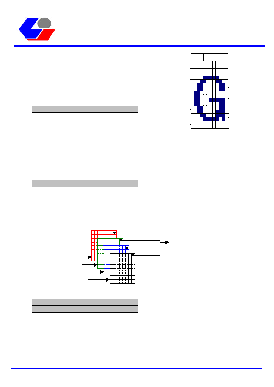
Architecture of OSD Font:
This Scaler IC provides 128 12*18 fonts downloadable; each font
Occupies 36 bytes of memory space, and the formula to calculate
Its No. mapped to the memory address is shown below:
Address = Font No. * 36
Font No. 0 to 127.
Font writing sequence:
WrFont
{0x5E}
1.
Calculate Font memory address.
2.
Set Font memory address. (write SetAdr {0x5B})
3.
Write 36 Bytes bit-map data into Font memory sequentially.
(write WrFont)
4.
if continue write next Font go to step.3
else go to step.1 set another Font No.
or stop procedure.
Set Multi-Color Font :
MultiColorFont[4:0]
{0x5A}
Set the Reg. to capture the color fonts; each color font occupies 4 monochrome fonts. If a color font is
increased,4 monochrome fonts available will be decreased. For example, when the Reg. is set to 2,2
color fonts can be used; The number of monochrome font starts from 8,the font No. 0 to 3 are mapped
to the same color font, and the font No. 4 to 7 are mapped to the same color font. The output of color
font is also mapped to the 24-bit color through the Color Pallet.
Set OSD Double Size :
DplH
{0x59[3]}
DplV
{0x59[2]}
Set the Reg. to enlarge the OSD horizontal or vertical direction twice, which has an effect only on the
font on the OSD (On-Screen Display) else than Border and Shadow on the OSD.
Font 4N
Font 4N+1
Font 4N+2
Font 4N+3
Combine to 4-bits color Font
Bit-0
Bit-1
Bit-2
Bit-3
0x00
0x02
0x04
0x06
0x08
0x0A
0x0C
0x0E
ROW-00
ROW-01
ROW-02
ROW-03
ROW-04
ROW-05
ROW-06
ROW-07
ROW-08
0x10
ROW-09
ROW-10
ROW-11
ROW-12
ROW-13
ROW-14
ROW-15
ROW-16
ROW-17
0x12
0x14
0x16
0x18
0x1A
0x1C
0x1E
0x20
0x22
Byte 0
Byte 1
lsb
msb
b
Font - N
0
7
0
3

Page 29 / 38
STK96C100
2.2.8 Contrast & Brightness Control
GainR[5:0]
{0x60}
GainG[5:0]
{0x61}
GainB[5:0]
{0x62}
DC[7:0]
{0x63}
GainR, GainG, and GainB respectively adjust the Contrast of OutputR, OutputG.and OutputB. The
value 32 is not adjusted; the Contrast will increase if the value is higher than 32,and the Contrast will
decrease if the value is lower than 32.The range of adjustment is from 0 to 63.
For DC[7:0], the brightness of OutputR,OutputG.and OutputB is adjusted. The range of adjustment is
from ≠127 to +127. In ASCII, 0x80 Brightness is the minimum, which goes up to 0xFF, 0x00
Brightness keeps constant, and 0x7F Brightness is the maximum.
2.2.9 Gamma Table Configuration
GammaWr[2:0]
{0x65[6:4]}
EnGamma
{0x65[3]}
SetGamma[7:0]
{0x66}
WrGamma[7:0]
{0x67}
This Scaler IC internally provides 3 256*8 bits RAM to serve as the Gamma-Correction for RGB. The
contents of Gamma Table can be input from up; the image data through the address of Gamma Table
can be converted into the mapped data output.
Program Gamma Table:
Requiring the program Gamma Table, up will first disable the function (EnGamma = 0) and then
decide which Gamma Table to write; the Gamma Table of RGB can be written in respectively or
together at the same time, and only the mapped GammaWr[2] = Blue, GammaWr[1] = Green, and
GammaWr[0] = Red must be set. The steps are shown as follows:
1.
Disable Gamma Correction. (EnGamma = 0)
2.
Set GammaWr to decide which one to program. (write GammaWr)
3.
Set SetGamma to decide which address to start program. (write SetGamma)
A[7:0]
DO[7:0]
MUX
From scaler
Image data
From uP ( SetGamma[7:0] )
MUX
To Dithering Control
DI[7:0]
From uP ( WrGamma[7:0] )

Page 30 / 38
STK96C100
4.
Write data into Gamma Table. (write WrGamma)
5.
If continuing to write the next address, go to step.4; else change another address and go to step.3,
or change another Gamma Table and go to step.2, or stop write Gamma Table go to step.6.
6. Enable Gamma Correction. (EnGamma = 1)
2.2.10 Dithering Control
EnDIT
{0x65[1]}
EnFRC
{0x65[2]}
Connecting the panel with minimum bit(s) (ex. the 18-bit panel), enable the function (EnDIT=1) to
simulate the 24-bit panel, and enable the dynamic Dithering (EnFRC=1) to enhance the effect of
Dithering.
2.2.11 Panel Border Color
BGC[5:0]
{0x64}
When the input video resolution is inferior to the output one and couldn't be enhanced as the output
video resolution, you can set the Reg. to change the panel border color not filled out by the input video.
In the Reg., bit [1:0], [3:2], [5:4] means the two maximum bits of RGB respectively; the other bits are
0.
2.2.12 Debug Mode
EnTest[7:0]
{0x0F}
Write Reg[0F] 0x60, 0x90, 0x60 in proper order to enter the Debug Mode. This moment, the internal
signal in this Scaler IC will be output to the Panel Odd Pixel output pins. Write the last Byte to select
which set of internal signals to output.
Mode
7
6
5
4
3
2
1
0
R EvenD[7] EvenD[6] OddD[23]
OddD[22]
OddD[15] OddD[14]
OddD[7]
OddD[6]
G
0
0
0
0
EvenD[23] EvenD[22] EvenD[15] EvenD[14]
1
B
HSIP
VSIP
CLP
LatCLK
DISP
DispH
DispV
0
R
IClrOV
0
0
EmptyH
EmptyV
0
0
PCLK
G
ExpH
ExpV
HCZ
VCZ
0
iEnRdH
iEnRdV
iClrOH
2
B
SyncH
SyncV
EnOUT
PHDE
PVDE
XDE
HXDE
VXDE
R iOSD_B[5] iOSD_B[4] iOSD_B[3] iOSD_B[2] iOSD_B[1] iOSD_B[0]
VCZ
HCZ
G iOSD_G[5] iOSD_G[4] iOSD_G[3] iOSD_G[2] iOSD_G[1] iOSD_G[0] iOSD_B[7] iOSD_B[6]
3
B iOSD_R[5] iOSD_R[4] iOSD_R[3] iOSD_R[2] iOSD_R[1] iOSD_R[0] iOSD_G[7] iOSD_G[6]
R DOUT[7] DOUT[6] DOUT[5]
DOUT[4]
DOUT[3] DOUT[2] DOUT[1] DOUT[0]
G iWVC[1]
iWVC[0]
iRVC[1]
iRVC[0]
DOUT[13] DOUT[22] DOUT[15] DOUT[14]
4
B IEnRdH
iEnRdV
iClrOH
iClrOV
PCLK
EmptyH
ExpH1
ExpV1
R POUT[7]
POUT[6]
POUT[5]
POUT[4]
POUT[3]
POUT[2]
POUT[1]
POUT[0]
G LatGPO
iMask
iSetPosEQ iNewMaxTog POUT[23] POUT[22] POUT[15] POUT[14]
5
B GmaAdr
GmaData iWrTbl[2]
iWrTbl[1]
iWrTbl[0]
iINC[2]
iINC[1]
iINC[0]

Page 31 / 38
STK96C100
2.3 Auto-Adjustment
2.3.1 Set Threshold
GateR[7:0]
{0x70}
GateG[7:0]
{0x71}
GateB[7:0]
{0x72}
Using the auto. Detecting circuit to adjust the input captured image, first set the Threshold of input
signal in the auto. Detecting circuit to avoid the noise affecting the operation of auto. Detecting
circuit.GateR, GateG, and GateB means the Threshold of Red, Green, and Blue input signal
respectively. The input signal level higher than the setting value will be allowed by the auto. Detecting
circuit.
2.3.2 Source Timing Measurement
HO
{0x80[1]}
2048 RefCLK
H-Sync missing
VO
{0x80[2]}
2048 Lines
V-Sync missing
HSP
{0x80[3]}
96/192 RefCLK H-Sync polarity
VSP
{0x80[4]}
32 Line
V-Sync polarity
HCT[11:0]
{0x82, 0x81}
RefCLK
Horizontal period
VCT[11:0]
{0x84, 0x83}
Line
Vertical period
HPOSL[10:0]
{0x88, 0x87}
VCLK
Horizontal display start
HPOSR[10:0]
{0x8A, 0x89}
VCLK
Horizontal display end
VSHC[11:0]
{0x86, 0x85}
VCLK
Interlace input detect
VPOS[7:0]
{0x8B}
Line
Vertical display start
The auto. Detecting circuit provides the following data for user's adjustment:
1.
HO: When the Flag is set to 1,no Hsync. input signal will show.
2.
VO: When the Flag is set to 1,no Vsync. input signal will show.
When the two Flags shown above is set to 1,0 to RstFlag {0x00[2]} can be written to clear
RstFlag .
3.
HSP: When the Flag is set to 0,the Hsync. input signal is positive; on the contrary, it is negative.
When the input signal is Composite during the period of Vsync., the Flag may be inaccurate.
4.
VSP: When the Flag is set to 0,the Vsync. input signal is positive; on the contrary, it is negative.
5.
HCT: The 12-bit value indicates the period of Hsync. input signal, RefCLK is the reference
frequency, and each front porch of Hsync. signal is updated.
6.
VCT: The 12-bit value indicates the count of the horizontal line of input signal; each Frame (the
front porch of Vsync. signal) is updated.
7.
HPOSL: The 11-bit value indicates the position of the left porch of input image, VCLK is the
reference frequency, and each Frame is updated.
t
Video
Level
GateX
t
0
1

Page 32 / 38
STK96C100
8.
HPOSR : The 11-bit value indicates the position of the right porch of input image, VCLK is the
reference frequency, and each Frame is updated.
9.
VSHC: The 12-bit value indicates that the horizontal scanning line emerges at the end of the
Hsync. while the input Vsync. signal emerges on the porch of the Vsync.. We can use the
data to determine if it is the Interlace signal and then determine if it is the Even or Odd
field. VCLK is the reference frequency; each Frame is updated.
10.
VPOS: The 8-bit value indicates the upper porch of input video, the number of horizontal scanning
line(HS) is the unit, and each Frame is updated.
2.3.3 Source Level Measurement
MinR[7:0]
{0x98}
MaxR[7:0]
{0x9B}
MinG[7:0]
{0x99}
MaxG[7:0]
{0x9C}
MinB[7:0]
{0x9A}
MaxB[7:0]
{0x9D}
The auto. Detecting circuit can detect the minimum and maximum of the input video data for the
Contrast adjustment of external ADC.
V-sync Pulse Width
Input
Sampling Area
HPOSL
HPOSR
H-sync Pulse Width
HCT
VCT
VPOS
HS
VS
VSHC

Page 33 / 38
STK96C100
When DetBlank ({0x77[7]}) = 0, the data in the image captured area will be detected;when DetBlank
= 1, all the data of input image will be detected.

Page 34 / 38
STK96C100
2.3.4 Source Clock Phase Measurement
The auto. Detecting circuit provides two methods shown below to detect if the frequency and phase of
input video are suitable.
TGX[11:0]
{0x91, 0x90}
TGY[11:0]
{0x93, 0x92}
TogRate[3:0]
{0x94}
LVD[15:0]
{0x96, 0x95}
EQC[4:0]
{0x97}
The auto. Detecting circuit can find which changing level of video data in the input video is more
frequent and then reveals its position (TGX, TGY) and its changing level (TogRate). With this
information, you can set the captured position (SetX, SetY) to capture the data of input video. 16
adjoin input video data (LVD) can be continuously captured in each Frame, and the video data
captured in the last Frame will be automatically compared. The result after compared will be put in
EQC. The Threshold set by GateR, GateG, and GateB will confine the video data captured.
Track[28:0]
{0xA1, 0xA0, 0x9F, 0x9E}
Slope
{0x77[5]}
GateDif[4:0]
{0x77[4:0]}
The other way provided by the auto. Detecting circuit is to count the variable of input video data. Two
parameters must be set: to select the changing direction (Slope) and to decide the Threshold (GateDif)
of changing slope (P7 or P8) when the condition meets the setting slope and the changing slope
Pn > GateDif, the changing slope (Pn) will be accumulated, and each Frame will be output to
Track.
2.3.5 Buffer Status Detection
SyncPosH[10:0]
{0xA3, 0xA2}
SyncPosV[10:0]
{0xA5, 0xA4}
PosSyncH[10:0]
{0xA7, 0xA6}
BufUsage[11:0]
{0xAC, 0xAB}
Over
{0x80[6]}
Under
{0x80[5]}
The auto. Detecting circuit detects the operation of internal Buffer, which offers the required information for
user
's reference to set the parameters.
1. SyncPosH: When the input video captured circuit dispatches a signal to require the output circuit to start
to output the image, the position of horizontal counter will be output. With the parameter, we
will know if the last output Hsync, signal is very close to the first output Hsync. signal to do
the necessary adjustment. The parameter depends on the output video (PCLK).
SetX[11:0]
{0x74, 0x73}
SetY[11:0]
{0x76, 0x75}
t
Video
Level
P1
P2
P3
P4
P5
P6
P7
P8
P7
P8
Slope = 1
Slope = 0

Page 35 / 38
STK96C100
2. SyncPosV: When the input video captured circuit dispatches a signal to require the output circuit to start
to output the image, the position of vertical counter will be output. When the last output
Hsync. signal is very close to the first output Hsync. signal, set the MaskPHS by way of the
parameter. The parameter depends on the count of output horizontal line.
3. PosSyncH: In the input Hsync. mode, the output horizontal period is controlled by the ratio of input
horizontal period.
For Duty of Output HS = SyncH = Duty of Input HS * RateV, we know that when the parameter
means SyncH, the position of horizontal counter will be output.
4.
BufUsage: The Buffer (3*1280*24 bits) with 3 horizontal lines long is provided within the Scaler
IC. This parameter indicates the maximum required by the Buffer in a Frame.
5.
Over: When the Flag is set to 1,the internal Buffer Overrun happens.(Write RstFlag=0 to clear the
Flag.)
6.
Under: When the Flag is set to 1, the internal Buffer Underrun Happens. (Write RstFlag=0 to
clear the Flag.)
Input VS
Input Video
Output DE
Output VS
Input HS
Output HS
SyncPosH
SyncPosV
Start output from this point
Last HS
First HS
PosSyncH
PHT
SyncH
Output DE
Output HS

Page 36 / 38
STK96C100
Page 37 / 38
STK96C100
Appendix A : List of Display Mode
01
640 x 350 @70
96
48
640
16
800
2
60
350
37
449
02
640 x 350 @85
64
96
640
32
832
3
60
350
32
445
03
640 x 400 @56
64
80
640
64
848
8
25
400
7
440
04
640 x 400 @70
64
80
640
16
800
2
34
400
13
449
05
640 x 400 @85
64
96
640
32
832
3
41
400
1
445
06
640 x 480 @60
96
48
640
16
800
2
33
480
10
525
07
640 x 480 @72
40
128
640
24
832
3
28
480
9
520
08
640 x 480 @75
64
120
640
16
840
3
16
480
1
500
09
640 x 480 @85
56
80
640
56
832
3
25
480
1
509
10
720 x 400 @70
108
54
720
18
900
2
35
400
12
449
11
720 x 400 @85
72
108
720
36
936
3
42
400
1
446
12
800 x 600 @56
72
128
800
24
1024
2
22
600
1
625
13
800 x 600 @60
128
88
800
40
1056
4
23
600
1
628
14
800 x 600 @72
120
64
800
56
1040
6
23
600
37
666
15
800 x 600 @75
80
160
800
16
1056
3
21
600
1
625
16
800 x 600 @85
64
152
800
32
1048
3
27
600
1
631
17
832 x 624 @75
64
244
832
32
1172
3
39
624
1
667
18
1024 x 768 @60
136
160
1024
24
1344
6
29
768
3
806
19
1024 x 768 @70
136
144
1024
24
1328
6
29
768
3
806
20
1024 x 768 @75
96
176
1024
16
1312
3
28
768
1
800
21
1024 x 768 @85
96
208
1024
48
1376
3
36
768
1
808
22
1152 x 864 @75
128
256
1152
64
1600
3
32
864
1
900
23
1152 x 864 @85
128
232
1152
64
1576
3
39
864
1
907
24
1152 x 870 @75
128
144
1152
132
1556
3
39
870
3
915
25
1280 x 960 @60
112
312
1280
96
1800
3
36
960
1
1000
26
1280 x 1024 @60
112
248
1280
48
1688
3
38
1024
1
1066
27
1280 x 1024 @75
144
248
1280
16
1688
3
38
1024
1
1066
28
1280 x 1024 @85
160
224
1280
64
1728
3
44
1024
1
1072
Unit : pixel
Unit : line
Horizontal
Vertical
Sync Back Display Front Total Sync Back Display Front Total
Width Porch Width Porch
Width Porch Size
Porch

Page 38 / 38
STK96C100
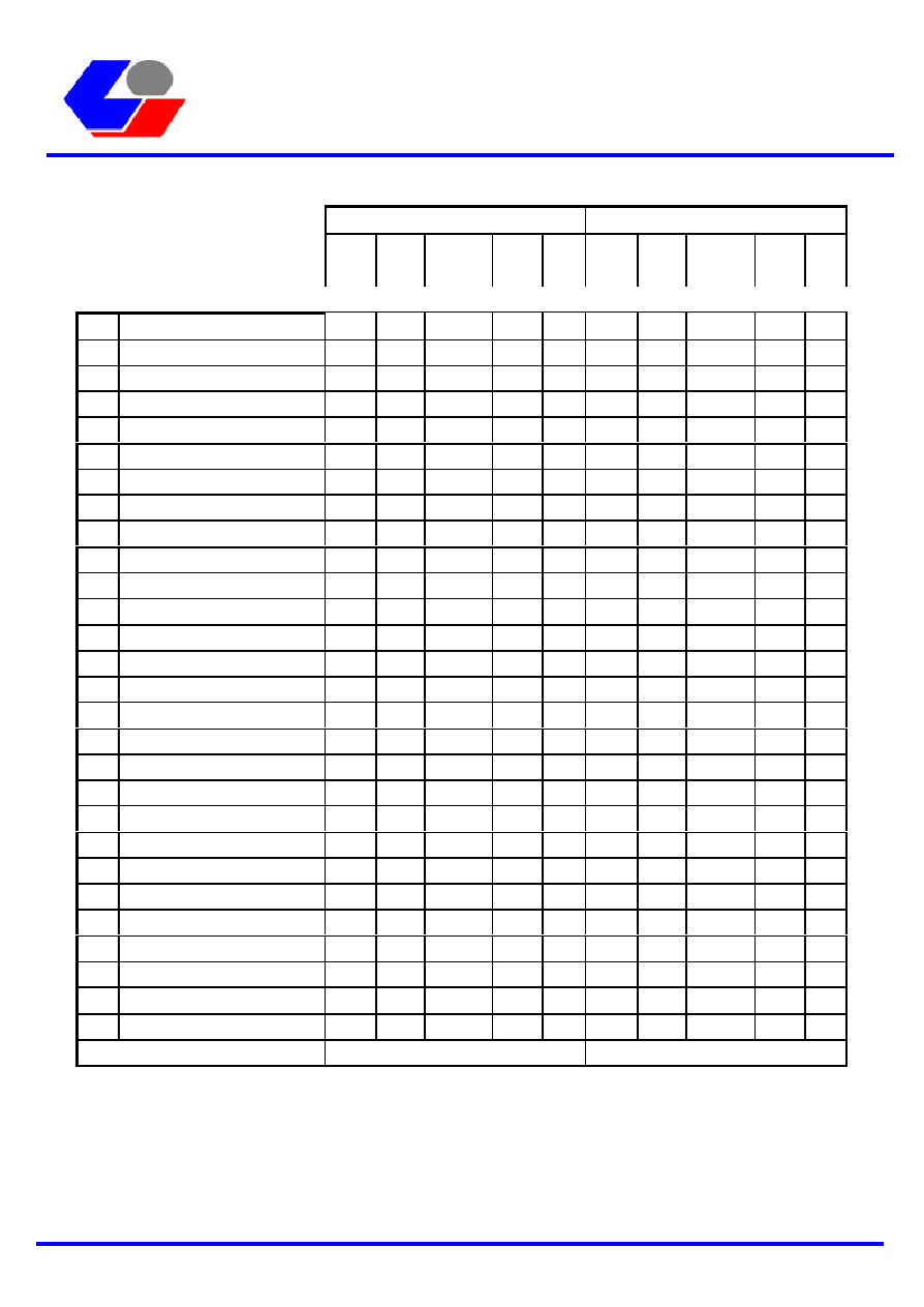
Appendix B : Quick Start
ADC : dual pixels parallel.
Input mode : 1024x768 @ 60Hz, H/V : -/-.
Output mode : 1024x768 @ 60Hz, DE/H/V : +/+/+.
Panel clock : internal PLL reference RefCLK = 14.318MHz.
GPIO[0:6] : input.
OSD : 40x5, center, border + shadow, default off.
Reg. Value Reg. Value Reg. Value Reg. Value Reg. Value Reg. Value Reg. Value
00
04
10
9D
20
18
30
03
40
00
50
0B
60
20
01
00
11
00
21
04
31
03
41
00
51
10
61
20
02
32
12
FF
22
A0
32
09
42
00
52
4E
62
20
03
6B
13
03
23
04
33
03
43
00
53
01
63
00
04
0A
14
1D
24
01
34
00
44
00
54
28
64
00
05
00
15
00
25
04
35
03
55
05
65
00
06
08
16
FF
26
01
36
00
56
2D
66
--
07
00
17
02
27
00
37
00
57
08
67
--
08
03
18
02
28
01
38
00
58
36
70
10
09
00
19
1E
29
04
39
03
59
00
71
10
0A
7F
1A
00
2A
41
3A
26
5A
00
72
10
0B
--
1B
01
2B
05
3B
03
5B
--
73
--
0C
--
1C
40
2C
00
5C
--
74
--
0D
--
1D
05
2D
FF
5D
--
75
--
0E
--
1E
00
2E
B9
5E
--
76
--
0F
--
2F
04
5F
--
77
04
After complete these registers setting, execute following steps to active Scaler IC.
Step1. : Send hardware reset pulse.
Step2. : Set Reg[02] to 0x02 to enable panel clock generator.
Step3. : Set Reg[00] to 0x07 to active scaler.
Step4. : Set Reg[01] to 0x3F to enable panel output.
Note(1) : don't hold hardware reset signal low during initial registers.
Note(2) : Set Reg[08] to 00, when there is no signals input, let output free run.
Note(3) : Set Reg[59] to 01 to enable OSD.