 | –≠–ª–µ–∫—Ç—Ä–æ–Ω–Ω—ã–π –∫–æ–º–ø–æ–Ω–µ–Ω—Ç: 10910 | –°–∫–∞—á–∞—Ç—å:  PDF PDF  ZIP ZIP |

Æ
1/7
MAIN PRODUCT APPLICATIONS:
EMI filtering and ESD protection for:
SIM Interface (Subscriber Identify Module)
UIM Interface (Universal Identify Module)
DESCRIPTION
The EMIF03-SIM01F2 is a highly integrated
devices designed to suppress EMI/RFI noise in all
systems subjected to electromagnetic interfer-
ences. The EMIF03 flip chip packaging means the
package size is equal to the die size.
This filter includes an ESD protection circuitry
which prevents the device from destruction when
subjected to ESD surges up 15kV.
BENEFITS
EMI symmetrical (I/O) low-pass filter
High efficiency in EMI filtering
Lead free package
Very low PCB space consuming:
1.42mm x 1.42mm
Very thin package: 0.65 mm
High efficiency in ESD suppression
High reliability offered by monolithic integration
High reducing of parasitic elements through
integration & wafer level packaging.
COMPLIES WITH THE FOLLOWING STANDARDS:
IEC61000-4-2
Level 4
15kV (air discharge)
8kV (contact discharge)
MIL STD 883E - Method 3015-6 Class 3
EMIF03-SIM01F2
3 LINES EMI FILTER
INCLUDING ESD PROTECTION
REV. 2
December 2004
Figure 2: Configuration
47
CLK in
Data in
CLK out
Data out
100
R1
R2
R3
RST in
RST out
100
V
CC
GND
Cline = 35pF max.
Flip-Chip
(8 Bumps)
Figure 1: Pin Configuration (Ball side)
B
C
1
2
3
A
RST
in
RST
out
CLT
in
Data
in
Gnd
V
CC
CLT
out
Data
out
TM: IPAD is a trademark of STMicroelectronics.
Table 1: Order Code
Part Number
Marking
EMIF03-SIM01F2
FC
IPADTM
EMIF03-SIM01F2
2/7
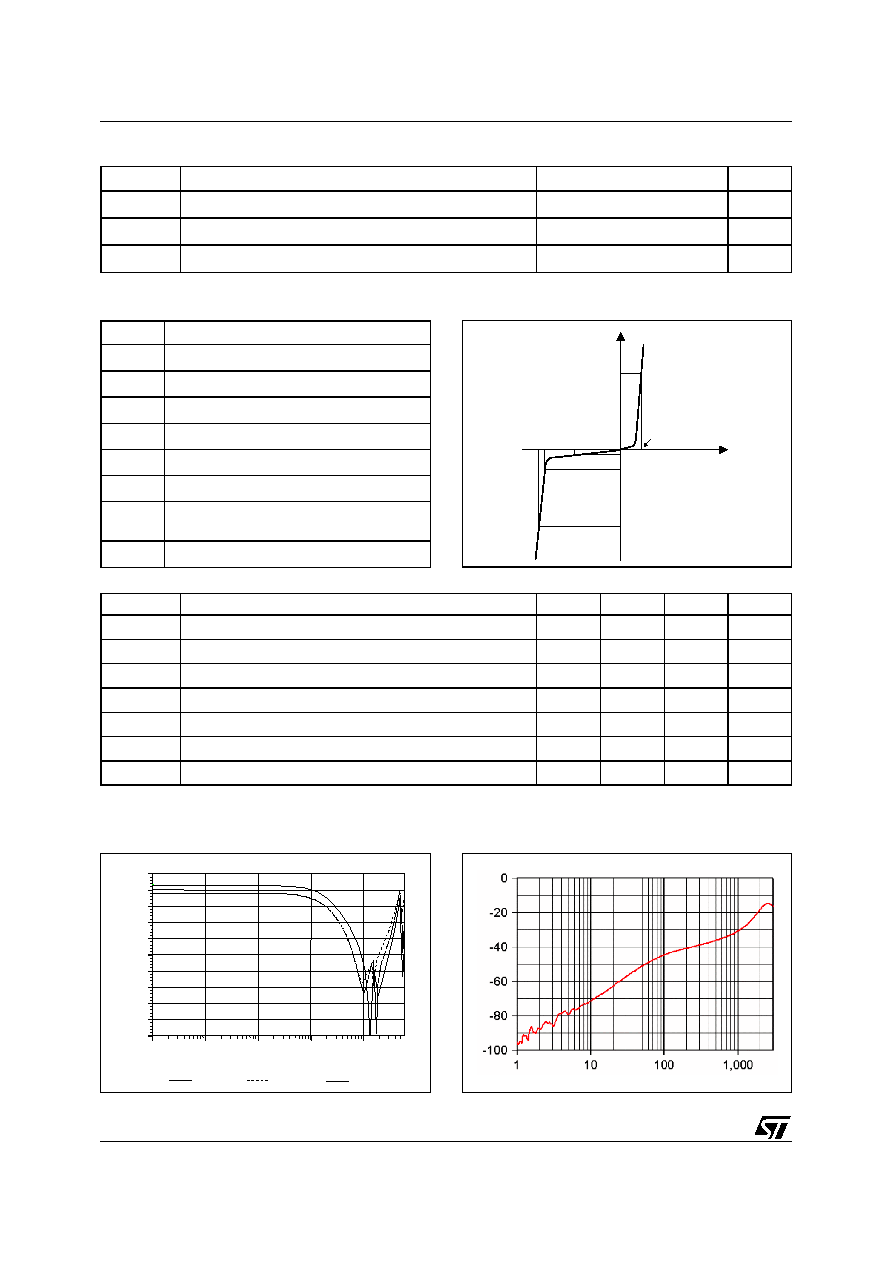
Table 2: Absolute Ratings (limiting values)
Table 3: Electrical Characteristics (T
amb
= 25∞C)
Symbol
Parameter and test conditions
Value
Unit
T
j
Maximum junction temperature
125
∞C
T
op
Operating temperature range
- 40 to + 85
∞C
T
stg
Storage temperature range
- 55 to + 150
∞C
Symbol
Parameter
V
BR
Breakdown voltage
I
RM
Leakage current @ V
RM
V
RM
Stand-off voltage
V
CL
Clamping voltage
R
d
Dynamic impedance
I
PP
Peak pulse current
R
I/O
Series resistance between Input &
Output
C
line
Input capacitance per line
Symbol
Test conditions
Min.
Typ.
Max.
Unit
V
BR
I
R
= 1 mA
6
V
I
RM
V
RM
= 3V per line
1
µA
R
d
1.5
R
1
95
100
105
R
2
44.65
47
49.35
R
3
95
100
105
C
line
@ 0V
35
pF
Figure 3: S21 (dB) attenuation measurement
Figure 4: Analog crosstalk measurements
Aplac 7.60 User: STMicroelectronics Feb 22 2001
100.0k
1.0M
10.0M
100.0M
1.0G
-50.00
-45.00
-40.00
-35.00
-30.00
-25.00
-20.00
-15.00
-10.00
-5.00
0.00
dB
f/Hz
B3_B1(CLK)
A3_A2(RST)
C3_C1(DAT)
dB
MHz
I
V
I
F
I
RM
I
R
I
PP
V
RM
V
F
V
BR
V
CL

EMIF03-SIM01F2
3/7
Figure 5:
Digital
crosstalk
measurement
Figure 6: ESD response to IEC61000-4-2
(+15kV air discharge) on one input V(in) and on
one output (Vout)
Figure 7: ESD response to IEC61000-4-2
(+15kV air discharge) on one input V(in) and on
one output (Vout)
Figure 8: Line capacitance versus applied
voltage (typical)
V(in1)
V(out1)
V(in1)
V(out1)
10
15
20
25
30
35
0
1
2
3
4
5
6
F=1MHz
Vosc=30mV
Tj=25∞C
C(pF)
VR(V)
EMIF03-SIM01F2
4/7
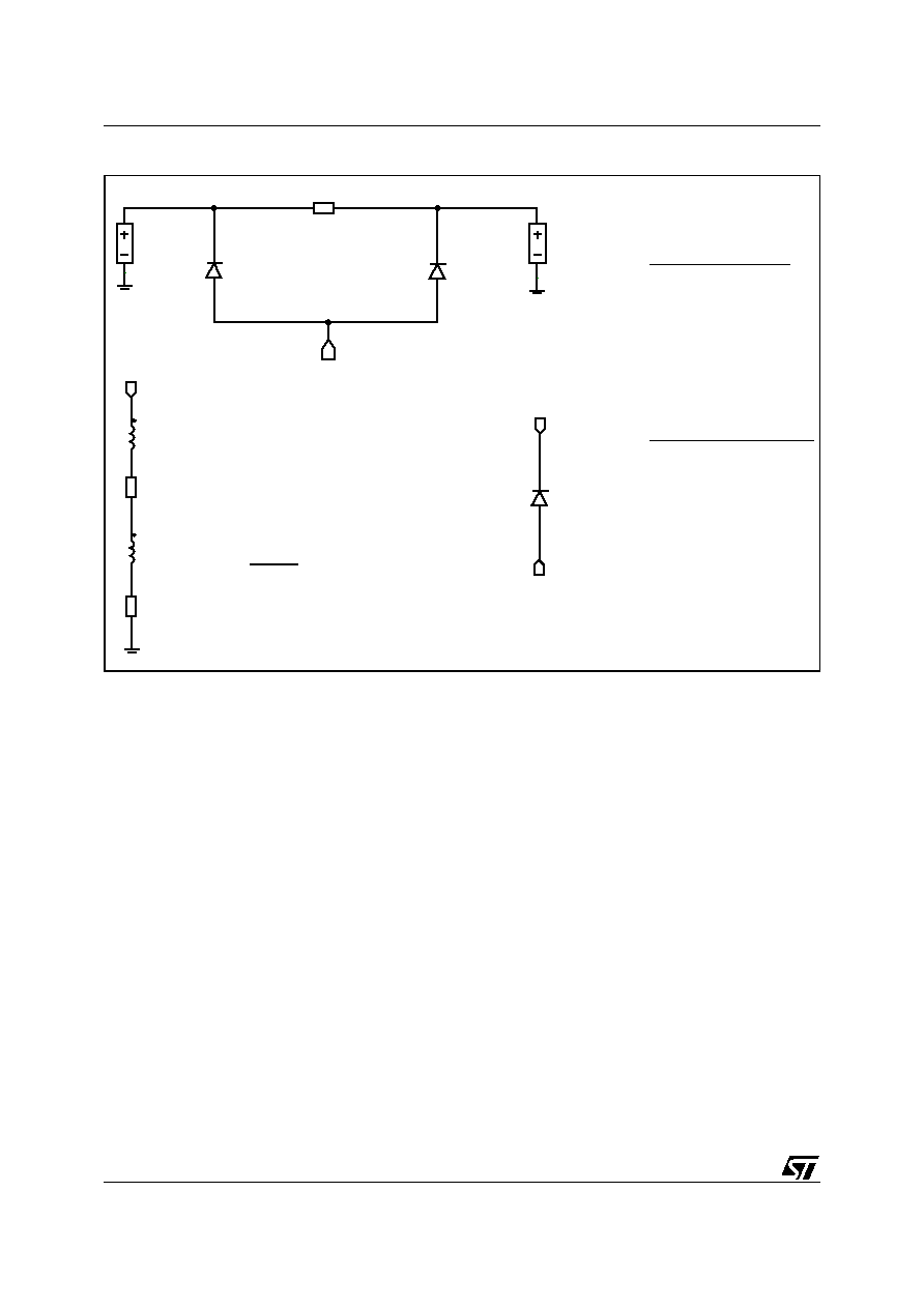
Figure 9: Aplac model
sub
50p
0.05
0.08nH
0.1
DEMIF03 diodes Model
- RS = 1.2
- CJO = 17p
- M = 0.3333
- VJ = 0.6
- ISR = 100p
- BV = 6.8
- IBV = 1m
- TT = 100n
Rseries = 47R (CLK line)
= 100R (RST & Data lines)
DEMIF03_Vcc diode Model
- RS = 1.5
- CJO = 20p
- M = 0.3333
- VJ = 0.6
- ISR = 100p
- BV = 6.8
- IBV = 1m
- TT = 100n
Rseries
sub
Port1
50
Port2
50
MODEL = demif03
MODEL = demif03
MODEL = demif03_Vcc
sub
Vcc

EMIF03-SIM01F2
5/7
Figure 10: Ordering Information Scheme
Figure 11: FLIP-CHIP Package Mechanical Data
Figure 12: Foot print recommendations
Figure 13: Marking
EMIF yy - xxx zz Fx
EMI Filter
Number of lines
Information
Package
x = resistance value (Ohms)
z = capacitance value / 10(pF)
or
3 letters = application
2 digits = version
F = Flip-Chip
x
= 1: 500µm, Bump = 315µm
= 2: Leadfree Pitch = 500µm, Bump = 315µm
= 3: Leadfree Pitch = 400µm, Bump = 250µm
1.42mm ± 50µm
1.42mm ± 50µm
315µm ± 50
500µm ± 50
5
00
µm ± 5
0
650µm ± 65
Copper pad Diameter :
250µm recommended , 300µm max
Solder stencil opening : 330µm
Solder mask opening recommendation :
340µm min for 315µm copper pad diameter
365
365
240
40
220
x
y
x
w
z
w
All dimensions in µm
E
Dot, ST logo
xx = marking
yww = datecode
(y = year
ww = week)
z = packaging
location