 | –≠–ª–µ–∫—Ç—Ä–æ–Ω–Ω—ã–π –∫–æ–º–ø–æ–Ω–µ–Ω—Ç: 1803DH | –°–∫–∞—á–∞—Ç—å:  PDF PDF  ZIP ZIP |

ST1803DHI
HIGH VOLTAGE FAST-SWITCHING
NPN POWER TRANSISTOR
s
NEW SERIES, ENHANCHED
PERFORMANCE
s
FULLY INSULATED PACKAGE FOR EASY
MOUNTING
s
INTEGRATED FREE WHEELING DIODE
s
HIGH VOLTAGE CAPABILITY
s
HIGH SWITCHING SPEED
s
TIGTHER hfe CONTROL
s
IMPROVED RUGGEDNESS
APPLICATIONS:
s
HORIZONTAL DEFLECTION FOR COLOR
TV
DESCRIPTION
The ST1803DHI is manufactured using Diffused
Collector technology for more stable operation Vs
base drive circuit variations resulting in very low
worst case dissipation.
Æ
INTERNAL SCHEMATIC DIAGRAM
January 2000
ABSOLUTE MAXIMUM RATINGS
Symbol
Parameter
Val ue
Uni t
V
CBO
Collector-Base Voltage (I
E
= 0)
1500
V
V
CEO
Collector-Emit ter Voltage (I
B
= 0)
600
V
V
EBO
Emitt er-Base Voltage (I
C
= 0)
7
V
I
C
Collector Current
10
A
I
CM
Collector Peak Current (t
p
< 5 ms)
15
A
I
B
Base Current
4
A
P
t ot
Total Dissipation at T
c
= 25
o
C
50
W
T
stg
St orage Temperature
-65 to 150
o
C
T
j
Max. Operating Junction T emperature
150
o
C
1
2
3
ISOWATT218
R
BE
=25
T yp.
1/6
THERMAL DATA
R
t hj-ca se
Thermal Resist ance Junction-case
Max
2.5
o
C/W
ELECTRICAL CHARACTERISTICS (T
case
= 25
o
C unless otherwise specified)
Symb ol
Parameter
Test Cond ition s
Mi n.
Typ .
Max.
Un it
I
CES
Collector Cut -of f
Current (V
BE
= 0)
V
CE
= 1500 V
V
CE
= 1500 V
T
j
= 125
o
C
1
2
mA
mA
I
EBO
Emitt er Cut -off Current
(I
C
= 0)
V
EB
= 4 V
130
400
mA
V
CE(sat )
Collector-Emit ter
Saturat ion Voltage
I
C
= 4 A
I
B
= 0. 8 A
I
C
= 4 A
I
B
= 1. 2 A
3
5
1.5
V
V
BE(s at)
Base-Emitt er
Saturat ion Voltage
I
C
= 4 A
I
B
= 0. 8 A
1.2
V
h
FE
DC Current G ain
I
C
= 1 A
V
CE
= 5 V
I
C
= 4. 5 A
V
CE
= 5 V
10
4
15
20
9
V
F
Diode F orward Voltage
I
F
= 5 A
1.5
2
V
BV
EB0
Emitt er-Breakdown
Voltage
I
E
= 700 mA
7
V
t
s
t
f
INDUCTIVE LOAD
St orage Time
Fall Time
I
C
= 4 A
I
Bon (END)
= 0.8 A
L
B
= 5
µ
H
V
BB
= -2.5 V
f = 16 KHz
5
0.3
6
0.6
µ
s
µ
s
Pulsed: Pulse duration = 300
µ
s, duty cycle 1.5 %
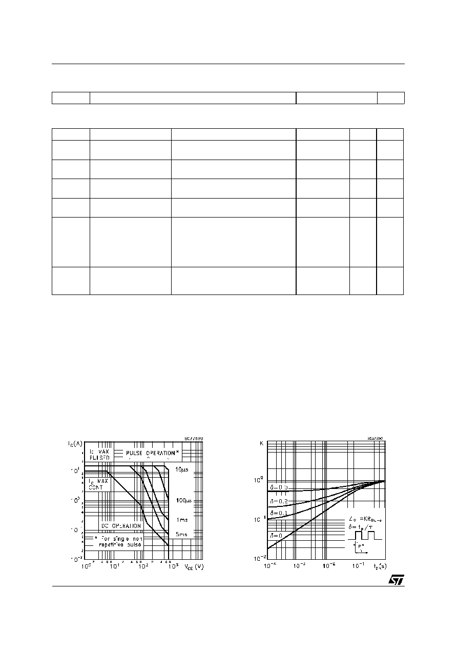
Safe Operating Area
Thermal Impedance
ST1803DHI
2/6

Derating Curve
Collector Emitter Saturation Voltage
Power Losses At 16 KHz
Biase Emitter Saturation Voltage
DC Current Gain
Switching Time Inductive Load
ST1803DHI
3/6
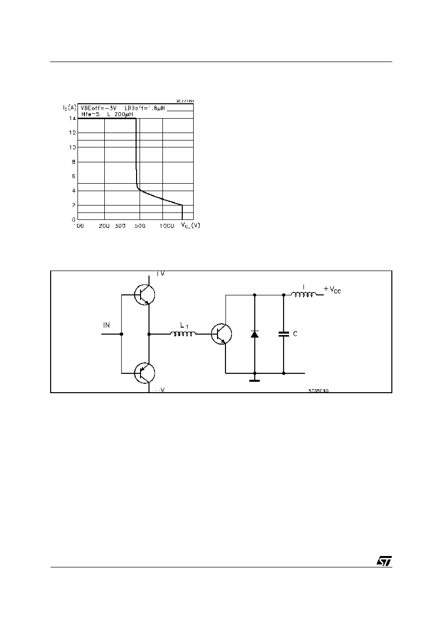
Reverse Biased SOA
Inductive Load Switching Test Circuits.
ST1803DHI
4/6

DIM.
mm
inch
MIN.
TYP.
MAX.
MIN.
TYP.
MAX.
A
5.35
5.65
0.211
0.222
C
3.30
3.80
0.130
0.150
D
2.90
3.10
0.114
0.122
D1
1.88
2.08
0.074
0.082
E
0.75
0.95
0.030
0.037
F
0.75
0.95
0.030
0.037
F2
1.50
1.70
0.059
0.067
F3
1.90
2.10
0.075
0.083
F5
1.10
0.043
G
10.80
11.20
0.425
0.441
H
15.80
16.20
0.622
0.638
L
9
0.354
L1
20.80
21.20
0.819
0.835
L2
19.10
19.90
0.752
0.783
L3
22.80
23.60
0.898
0.929
L4
40.50
42.50
1.594
1.673
L5
4.85
5.25
0.191
0.207
L6
20.25
20.75
0.797
0.817
N
2.1
2.3
0.083
0.091
R
4.6
0.181
DIA
3.5
3.7
0.138
0.146
P025C/B
ISOWATT218 NARROW LEADS MECHANICAL DATA
- Weight : 4.9 g (typ.)
- Maximum Torque (applied to mounting flange) Recommended: 0.8 Nm; Maximum: 1 Nm
- The side of the dissipator must be flat within 80
µ
m
ST1803DHI
5/6