 | –≠–ª–µ–∫—Ç—Ä–æ–Ω–Ω—ã–π –∫–æ–º–ø–æ–Ω–µ–Ω—Ç: 27C1024 | –°–∫–∞—á–∞—Ç—å:  PDF PDF  ZIP ZIP |

M27C1024
1 Mbit (64Kb x16) UV EPROM and OTP EPROM
September 1998
1/15
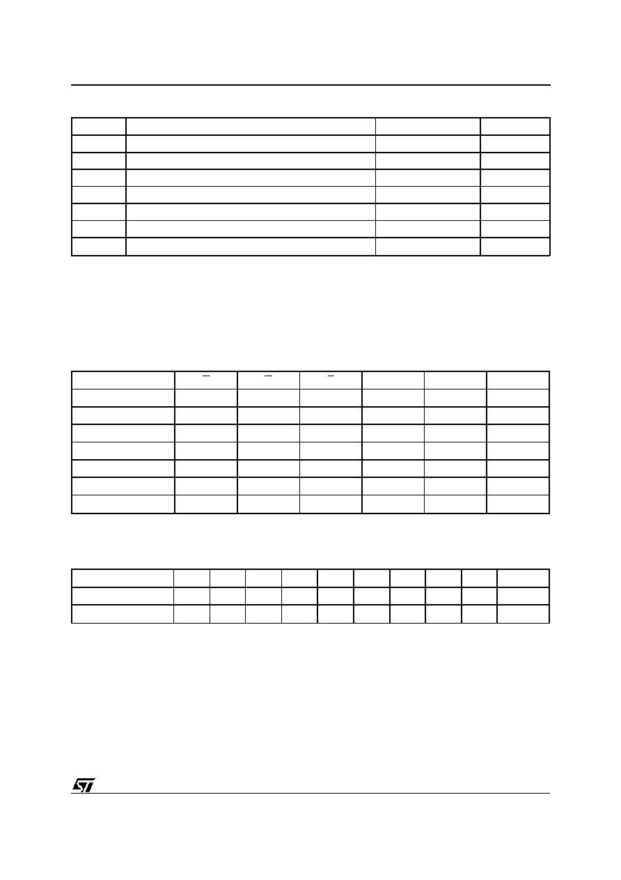
AI00702B
16
A0-A15
P
Q0-Q15
VPP
VCC
M27C1024
G
E
VSS
16
Figure 1. Logic Diagram
5V
±
10% SUPPLY VOLTAGE in READ
OPERATION
FAST ACCESS TIME: 35ns
LOW POWER CONSUMPTION:
≠ Active Current 35mA at 5MHz
≠ Standby Current 100
µ
A
PROGRAMMING VOLTAGE: 12.75V
±
0.25V
PROGRAMMING TIME: 100
µ
s/byte (typical)
ELECTRONIC SIGNATURE
≠ Manufacturer Code: 0020h
≠ Device Code: 008Ch
DESCRIPTION
The M27C1024 is a 1 Mbit EPROM offered in the
two ranges UV (ultra violet erase) and OTP (one
time programmable). It is ideally suited for micro-
processor systems requiring large data or program
storage and is organized as 65,536 words of 16
bits.
The FDIP40W (window ceramic frit-seal package)
has a transparent lid which allows the user to
expose the chip to ultraviolet light to erase the bit
pattern. A new pattern can then be written to the
device by following the programming procedure.
For application where the content is programmed
only one time and erasure is not required, the
M27C1024 is offered in PDIP40, PLCC44 and
TSOP40 (10 x 14mm) packages.
A0-A15
Address Inputs
Q0-Q15
Data Outputs
E
Chip Enable
G
Output Enable
P
Program
V
PP
Program Supply
V
CC
Supply Voltage
V
SS
Ground
Table 1. Signal Names
1
40
FDIP40W (F)
PLCC44 (C)
TSOP40 (N)
10 x 14mm
1
40
PDIP40 (B)

Q6
Q5
Q4
Q11
Q8
VSS
Q7
Q10
Q9
A12
A8
A11
A10
A6
A13
A9
VSS
A7
A2
Q1
Q0
A0
G
A1
A5
NC
P
E
Q12
VPP
VCC
Q15
AI00703
M27C1024
8
1
2
3
4
5
6
7
9
10
11
12
13
14
15
16
32
31
30
29
28
27
26
25
24
23
22
21
20
19
18
17
Q3
Q2
Q14
Q13
A4
A3
40
39
38
37
36
35
34
33
A14
A15
Figure 2A. DIP Pin Connections
AI00704
A14
A11
A7
A3
23
Q6
Q5
Q4
Q3
Q2
NC
A2
Q12
Q8
VSS
NC
Q11
Q10
12
A15
A9
1
Q15
VSS
A12
Q13
A5
44
NC
NC
M27C1024
Q14
A13
A4
NC
A6
34
Q1
Q9
A10
A8
Q7
Q0
G
A0
A1
V
PP
E
P
V
CC
Figure 2B. LCC Pin Connections
Warning: NC = Not Connected.
DEVICE OPERATION
The modes of operations of the M27C1024 are
listed in the Operating Modes table. A single power
supply is required in the read mode. All inputs are
TTL levels except for Vpp and 12V on A9 for
Electronic Signature.
Read Mode
The M27C1024 has two control functions, both of
which must be logically active in order to obtain
data at the outputs. Chip Enable (E) is the power
control and should be used for device selection.
Output Enable (G) is the output control and should
be used to gate data to the output pins, inde-
pendent of device selection. Assuming that the
addresses are stable, the address access time
(t
AVQV
) is equalto the delay from E to output (t
ELQV
).
Data is available at the output after a delay of t
OE
from the falling edge of G, assuming that E has
been low and the addresses have been stable for
at least t
AVQV
-t
GLQV
.
Standby Mode
The M27C1024 has a standby mode which re-
duces the active current from 35mA to 100
µ
A.
The M27C1024 is placed in the standby mode by
applying a TTL high signal to the E input. When in
the standby mode, the outputs are in a high imped-
ance state, independent of the G input.
Warning: NC = Not Connected.
DQ6
DQ3
DQ2
DQ13
DQ8
DQ7
DQ10
DQ9
A14
A8
A11
A10
A4
A15
A9
G
A7
A2
DQ1
DQ0
A0
A1
A3
NC
P
E
DQ14
VPP
VCC
DQ15
AI01582
M27C1024
(Normal)
10
1
11
20
21
30
31
40
VSS
A12
A6
A13
A5
DQ12
DQ4
DQ11
DQ5
VSS
Figure 2C. TSOP Pin Connections
Warning: NC = Not Connected.
2/15
M27C1024
Symbol
Parameter
Value
Unit
T
A
Ambient Operating Temperature
(3)
≠40 to 125
∞
C
T
BIAS
Temperature Under Bias
≠50 to 125
∞
C
T
STG
Storage Temperature
≠65 to 150
∞
C
V
IO
(2)
Input or Output Voltages (except A9)
≠2 to 7
V
V
CC
Supply Voltage
≠2 to 7
V
V
A9
(2)
A9 Voltage
≠2 to 13.5
V
V
PP
Program Supply Voltage
≠2 to 14
V
Notes: 1. Except for the rating "Operating Temperature Range", stresses above those listed in the Table "Absolute Maximum Ratings"
may cause permanent damage to the device. These are stress ratings only and operation of the device at these or any other
conditions above those indicated in the Operating sections of this specification is not i mplied. Exposure to Absolute Maximum
Rating conditions for extended periods may affect device reliability. Refer also to the STMicroelectronics SURE Program and other
relevant quality documents.
2. Minimum DC voltage on Input or Output is ≠0.5V with possible undershoot to ≠2.0V for a period less than 20ns. Maximum DC
voltage on Output is V
CC
+0.5V with possible overshoot to V
CC
+2V for a period less than 20ns.
3. Depends on range.
Table 2. Absolute Maximum Ratings
(1)
Mode
E
G
P
A9
V
PP
Q0 - Q15
Read
V
IL
V
IL
V
IH
X
V
CC
or V
SS
Data Output
Output Disable
V
IL
V
IH
X
X
V
CC
or V
SS
Hi-Z
Program
V
IL
X
V
IL
Pulse
X
V
PP
Data Input
Verify
V
IL
V
IL
V
IH
X
V
PP
Data Output
Program Inhibit
V
IH
X
X
X
V
PP
Hi-Z
Standby
V
IH
X
X
X
V
CC
or V
SS
Hi-Z
Electronic Signature
V
IL
V
IL
V
IH
V
ID
V
CC
Codes
Note: X = V
IH
or V
IL
, V
ID
= 12V
±
0.5V
Table 3. Operating Modes
Identifier
A0
Q7
Q6
Q5
Q4
Q3
Q2
Q1
Q0
Hex Data
Manufacturer's Code
V
IL
0
0
1
0
0
0
0
0
20h
Device Code
V
IH
1
0
0
0
1
1
0
0
8Ch
Note: Outputs Q8-Q15 are set to '0'.
Table 4. Electronic Signature
3/15
M27C1024
AI01822
3V
High Speed
0V
1.5V
2.4V
Standard
0.4V
2.0V
0.8V
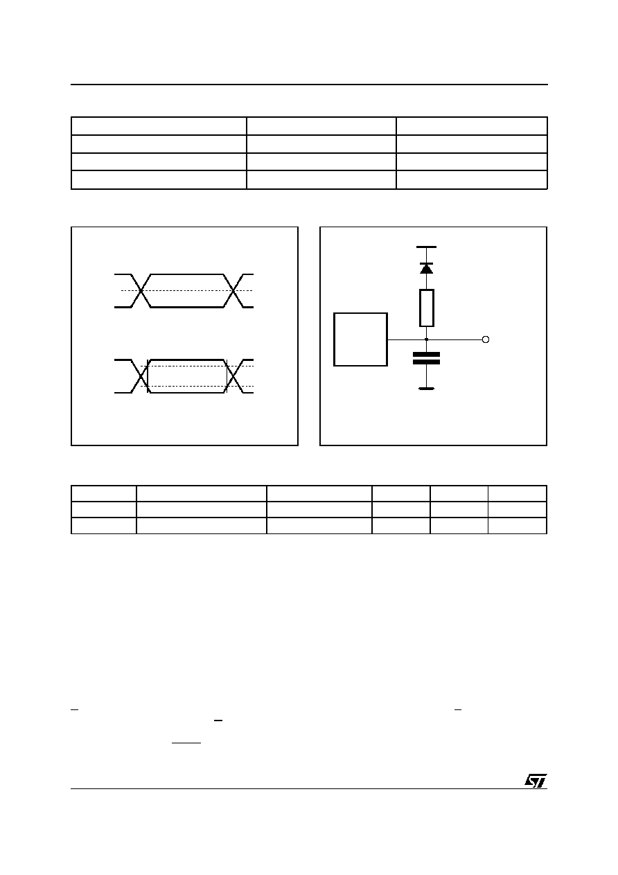
Figure 3. AC Testing Input Output Waveform
AI01823B
1.3V
OUT
CL
CL = 30pF for High Speed
CL = 100pF for Standard
CL includes JIG capacitance
3.3k
1N914
DEVICE
UNDER
TEST
Figure 4. AC Testing Load Circuit
High Speed
Standard
Input Rise and Fall Times
10ns
20ns
Input Pulse Voltages
0 to 3V
0.4V to 2.4V
Input and Output Timing Ref. Voltages
1.5V
0.8V and 2V
Table 5. AC Measurement Conditions
Symbol
Parameter
Test Condition
Min
Max
Unit
C
IN
Input Capacitance
V
IN
= 0V
6
pF
C
OUT
Output Capacitance
V
OUT
= 0V
12
pF
Note: 1. Sampled only, not 100% tested.
Table 6. Capacitance
(1)
(T
A
= 25
∞
C, f = 1 MHz )
Two Line Output Control
BecauseEPROMs are usually used in largermem-
ory arrays, this product features a 2 line control
function which accommodates the use of multiple
memory connection. The two line control function
allows:
a. the lowest possible memory power dissipation,
b. complete assurance that output bus contention
will not occur.
For the most efficient use of thesetwo control lines,
E should be decoded and used as the primary
device selecting function, while G should be made
a common connection to all devices in the array
and connected to the READ line from the system
control bus. This ensures that all deselected mem-
ory devices are in their low power standby mode
and that the output pins are only active when data
is required from a particular memory device.
System Considerations
The power switching characteristics of Advanced
CMOS EPROMs require careful decoupling of the
devices. The supply current, I
CC
, has three seg-
ments that are of interest to the system designer :
the standby current level, the active current level,
and transient current peaks that are produced by
the falling and rising edges of E. The magnitude of
transientcurrent peaks is dependenton the capaci-
tive and inductive loading of the device at the
output.
4/15
M27C1024

Symbol
Parameter
Test Condition
Min
Max
Unit
I
LI
Input Leakage Current
0V
V
IN
V
CC
±
10
µ
A
I
LO
Output Leakage Current
0V
V
OUT
V
CC
±
10
µ
A
I
CC
Supply Current
E = V
IL
, G = V
IL
,
I
OUT
= 0mA, f = 5MHz
35
mA
I
CC1
Supply Current (Standby) TTL
E = V
IH
1
mA
I
CC2
Supply Current (Standby) CMOS
E > V
CC
≠ 0.2V
100
µ
A
I
PP
Program Current
V
PP
= V
CC
100
µ
A
V
IL
Input Low Voltage
≠0.3
0.8
V
V
IH
(2)
Input High Voltage
2
V
CC
+ 1
V
V
OL
Output Low Voltage
I
OL
= 2.1mA
0.4
V
V
OH
Output High Voltage TTL
I
OH
= ≠400
µ
A
2.4
V
Output High Voltage CMOS
I
OH
= ≠100
µ
A
V
CC
≠ 0.7
V
Notes: 1. V
CC
must be applied simultaneously with or before V
PP
and removed simultaneously with or after V
PP.
2. Maximum DC voltage on Output is V
CC
+0.5V.
Table 7. Read Mode DC Characteristics
(1)
(T
A
= 0 to 70
∞
C, ≠40 to 85
∞
C; ≠40 to 105
∞
C or ≠40 to 125
∞
C; V
CC
= 5V
±
5% or 5V
±
10%; V
PP
= V
CC
)
Symbol
Alt
Parameter
Test Condition
M27C1024
Unit
-35
(3)
-45
(3)
-55
(3)
Min
Max
Min
Max
Min
Max
t
AVQV
t
ACC
Address Valid to Output Valid
E = V
IL
, G = V
IL
35
45
55
ns
t
ELQV
t
CE
Chip Enable Low to Output Valid
G = V
IL
35
45
55
ns
t
GLQV
t
OE
Output Enable Low to Output Valid
E = V
IL
20
25
30
ns
t
EHQZ
(2)
t
DF
Chip Enable High to Output Hi-Z
G = V
IL
0
30
0
30
0
30
ns
t
GHQZ
(2)
t
DF
Output Enable High to Output Hi-Z
E = V
IL
0
30
0
30
0
30
ns
t
AXQX
t
OH
Address Transition to Output
Transition
E = V
IL
, G = V
IL
0
0
0
ns
Notes: 1. V
CC
must be applied simultaneously with or before V
PP
and removed simultaneously with or after V
PP.
2. Sampled only, not 100% tested.
3. Speed obtained with High Speed AC measurement conditions.
Table 8A. Read Mode AC Characteristics
(1)
(T
A
= 0 to 70
∞
C, ≠40 to 85
∞
C; ≠40 to 105
∞
C or ≠40 to 125
∞
C; V
CC
= 5V
±
5% or 5V
±
10%; V
PP
= V
CC
)
5/15
M27C1024