 | –≠–ª–µ–∫—Ç—Ä–æ–Ω–Ω—ã–π –∫–æ–º–ø–æ–Ω–µ–Ω—Ç: 27L2C | –°–∫–∞—á–∞—Ç—å:  PDF PDF  ZIP ZIP |

1/9
s
VERY LOW POWER CONSUMPTION :
10µA/op
s
OUTPUT VOLTAGE CAN SWING TO
GROUND
s
EXCELLENT PHASE MARGIN ON
CAPACITIVE LOADS
s
STABLE AND LOW OFFSET VOLTAGE
s
THREE INPUT OFFSET VOLTAGE
SELECTIONS
DESCRIPTION
These devices are low cost, low power dual oper-
ational amplifiers designed to operate with single
or dual supplies. These operational amplifiers use
the ST silicon gate CMOS process allowing an ex-
cellent consumption-speed ratio. These series are
ideally suited for low consumption applications.
Three power consumptions are available allowing
to have always the best consumption-speed ratio:
u
I
CC
= 10µA/amp.: TS27L2 (very low power)
u
I
CC
= 150µA/amp.: TS27M2 (low power)
u
I
CC
= 1mA/amp.: TS272 (standard)
These CMOS amplifiers offer very high input im-
pedance and extremely low input currents. The
major advantage versus JFET devices is the very
low input currents drift with temperature (see fig-
ure 2).
ORDER CODE
N = Dual in Line Package (DIP)
D = Small Outline Package (SO) - also available in Tape & Reel (DT)
P = Thin Shrink Small Outline Package (TSSOP) - only available
in Tape & Reel (PT)
PIN CONNECTIONS (top view)
Part Number
Temperature Range
Package
N
D
P
TS27L2C/AC/BC
0∞C, +70∞C
∑
∑
∑
TS27L2I/AI/BI
-40∞C, +125∞C
∑
∑
∑
TS27L2M/AM/BM
-55∞C, +125∞C
∑
∑
∑
Example : TS27L2ACN
N
DIP8
(Plastic Package)
D
SO8
(Plastic Micropackage)
P
TSSOP8
(Thin Shrink Small Outline Package)
1
2
3
4
5
6
7
8
CC
+
-
-
+
-
+
CC
1 - Output 1
2 - Inverting Input 1
3 - Non-inverting Input 1
4 - V
5 - Non-inverting Input 2
6 - Inverting Input 2
7 - Output 2
8 - V
TS27L2C,I,M
PRECISION VERY LOW POWER
CMOS DUAL OPERATIONAL AMPLIFIERS
November 2001

TS27L2C,I,M
2/9
BLOCK DIAGRAM
ABSOLUTE MAXIMUM RATINGS
OPERATING CONDITIONS
E
E
Input
differential
Second
stage
Output
stage
Output
CC
V
CC
V
Current
source
x I
Symbol
Parameter
TS27L2C/AC/BC
TS27L2I/AI/BI
TS27L2M/AM/BM
Unit
V
CC
+
Supply Voltage
1)
18
V
V
id
Differential Input Voltage
2)
±18
V
V
i
Input Voltage
3)
-0.3 to 18
V
I
o
Output Current for V
CC
+
15V
±30
mA
I
in
Input Current
±5
mA
T
oper
Operating Free-Air Temperature Range
0 to +70
-40 to +125
-55 to +125
∞C
T
stg
Storage Temperature Range
-65 to +150
∞C
1. All values, except differential voltage are with respect to network ground terminal.
2. Differential voltages are the non-inverting input terminal with respect to the inverting input terminal.
3. The magnitude of the input and the output voltages must never exceed the magnitude of the positive supply voltage.
Symbol
Parameter
Value
Unit
V
CC
+
Supply Voltage
3 to 16
V
V
icm
Common Mode Input Voltage Range
0 to V
CC
+
- 1.5
V

TS27L2C,I,M
3/9
SCHEMATIC DIAGRAM (for 1/2 TS27L2)
T
T
25
2
T
17
18
R
T
20
T
21
T
T
23
22
In
p
u
t
Out
p
u
t
T
24
T
19
V
CC
V
CC
T
26
T
27
T
28
T
29
In
p
u
t
T
3
T
4
T
5
T
2
T
1
R1
C1
T
7
T
6
T
8
T
9
T
13
T
14
T
11
T
12
T
10
T
16
T
15

TS27L2C,I,M
4/9
ELECTRICAL CHARACTERISTICS
V
CC
+
= +10V, V
CC
-
= 0V, T
amb
= +25∞C (unless otherwise specified)
Symbol
Parameter
TS27L2C/AC/BC
TS27L2I/AI/BI
TS27L2M/AM/BM
Unit
Min.
Typ.
Max.
Min.
Typ.
Max.
V
io
Input Offset Voltage
V
O
= 1.4V, V
ic
= 0V
TS27L2C/I/M
TS27L2AC/AI/AM
TS27L2B/C/I/M
T
min
T
amb
T
max
TS27L2C/I/M
TS27L2AC/AI/AM
TS27L2B/C/I/M
1.1
0.9
0.25
10
5
2
12
6.5
3
1.1
0.9
0.25
10
5
2
12
6.5
3.5
mV
DV
io
Input Offset Voltage Drift
2
2
µV/∞C
I
io
Input Offset Current note
1)
V
ic
= 5V, V
O
= 5V
T
min
T
amb
T
max
1.
Maximum values including unavoidable inaccuracies of the industrial test.
1
100
1
200
pA
I
ib
Input Bias Current - see note 1
V
ic
= 5V, V
O
= 5V
T
min
T
amb
T
max
1
150
1
300
pA
V
OH
High Level Output Voltage
V
id
= 100mV, R
L
= 1M
T
min
T
amb
T
max
8.8
8.7
9
8.8
8.6
9
V
V
OL
Low Level Output Voltage
V
id
= -100mV
50
50
mV
A
vd
Large Signal Voltage Gain
V
iC
= 5V, R
L
= 1M
,
V
o
= 1V to 6V
T
min
T
amb
T
max
60
45
100
60
40
100
V/mV
GBP
Gain Bandwidth Product
A
v
= 40dB, R
L
= 1M
,
C
L
= 100pF, f
in
= 100kHz
0.1
0.1
MHz
CMR
Common Mode Rejection Ratio
V
iC
= 1V to 7.4V, V
o
= 1.4V
65
80
65
80
dB
SVR
Supply Voltage Rejection Ratio
V
CC
+
= 5V to 10V, V
o
= 1.4V
60
80
60
80
dB
I
CC
Supply Current (per amplifier)
A
v
= 1, no load, V
o
= 5V
T
min
T
amb
T
max
10
15
17
10
15
18
µA
I
o
Output Short Circuit Current
V
o
= 0V, V
id
= 100mV
60
60
mA
I
sink
Output Sink Current
V
o
= V
CC
, V
id
= -100mV
45
45
mA
SR
Slew Rate at Unity Gain
R
L
= 1M
, C
L
= 100pF, V
i
= 3 to 7V
0.04
0.04
V/
µ
s
m
Phase Margin at Unity Gain
A
v
= 40dB, R
L
= 1M
, C
L
= 100pF
45
45
Degrees
K
OV
Overshoot Factor
30
30
%
e
n
Equivalent Input Noise Voltage
f = 1kHz, R
s
= 100
68
68
V
o1
/V
o2
Channel Separation
120
120
dB
nV
Hz
------------
TS27L2C,I,M
5/9
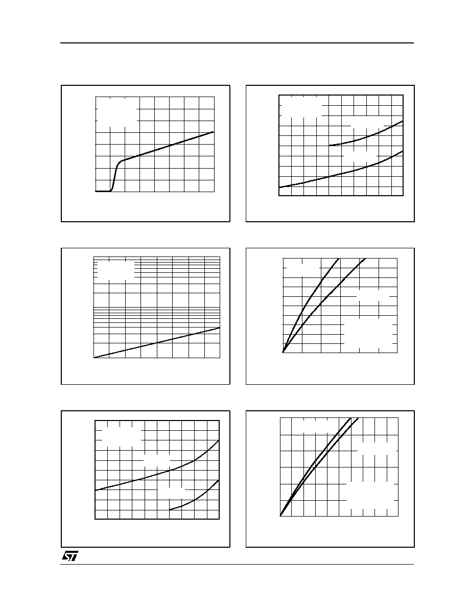
TYPICAL CHARACTERISTICS
Figure 1 : Supply Current (each amplifier) versus
Supply Voltage
Figure 2 : Input Bias Current versus Free Air
Temperature
Figure 3a : High Level Output Voltage versus
High Level Output Current
Figure 3b : High Level Output Voltage versus
High Level Output Current
Figure 4a : Low Level Output Voltage versus Low
Level Output Current
Figure 4b : Low Level Output Voltage versus Low
Level Output Current
CC
SUPPLY VOLTAGE, V
(V)
CC
amb
V
O
CC
∞
0
4
8
12
16
20
µ
S
U
PPL
Y
C
U
RRE
NT,
I
(
A
)
T
= 25 C
A = 1
V = V
/ 2
15
10
5
25
50
75
100
125
amb
I
N
P
U
T
B
I
A
S
CUR
RE
NT,
I
(
p
A
)
IB
TEMPERATURE, T
( C)
∞
V
= 10V
V = 5V
CC
i
100
10
1
5
4
3
2
1
0
-10
-8
-6
-4
-2
0
OH
OUTPUT CURRENT, I
(mA)
O
U
T
P
U
T
VO
LT
A
G
E,
V
(
V
)
OH
amb
id
T
= 25 C
V
= 100mV
∞
V
= 5V
V
= 3V
CC
CC
20
16
12
8
4
0
-50
-40
-30
-20
-10
0
amb
id
∞
T
= 25 C
V
= 100mV
V
= 16V
CC
CC
V
= 10V
OUTPUT CURRENT, I
(mA)
OH
OH
O
U
T
P
U
T
V
O
L
T
AG
E
,
V
(
V)
1 .0
0 .8
0 .6
0 .4
0 .2
amb
ic
id
T
= 2 5 ∞C
V
= 0 .5 V
V
= -1 0 0 m V
V
= 3 V
V
= 5 V
C C
C C
OL
O
U
T
P
U
T
V
O
L
T
AG
E,
V
(V
)
0
1
2
3
O U T P U T C U R R E N T , I
(m A )
O L
0
4
8
1 2
1 6
2 0
O
U
T
P
U
T
V
O
L
T
AG
E,
V
(
V)
OL
amb
id
i
T
= 2 5 ∞C
V = 0 .5 V
V
= -1 0 0 m V
C C
V
= 1 0 V
C C
V
= 1 6 V
O U T P U T C U R R E N T , I
(m A )
OL
3
2
1