 | –≠–ª–µ–∫—Ç—Ä–æ–Ω–Ω—ã–π –∫–æ–º–ø–æ–Ω–µ–Ω—Ç: 2N1893 | –°–∫–∞—á–∞—Ç—å:  PDF PDF  ZIP ZIP |
2N1893
October 1988
GENERAL PURPOSE HIGH-VOLTAGE TYPE
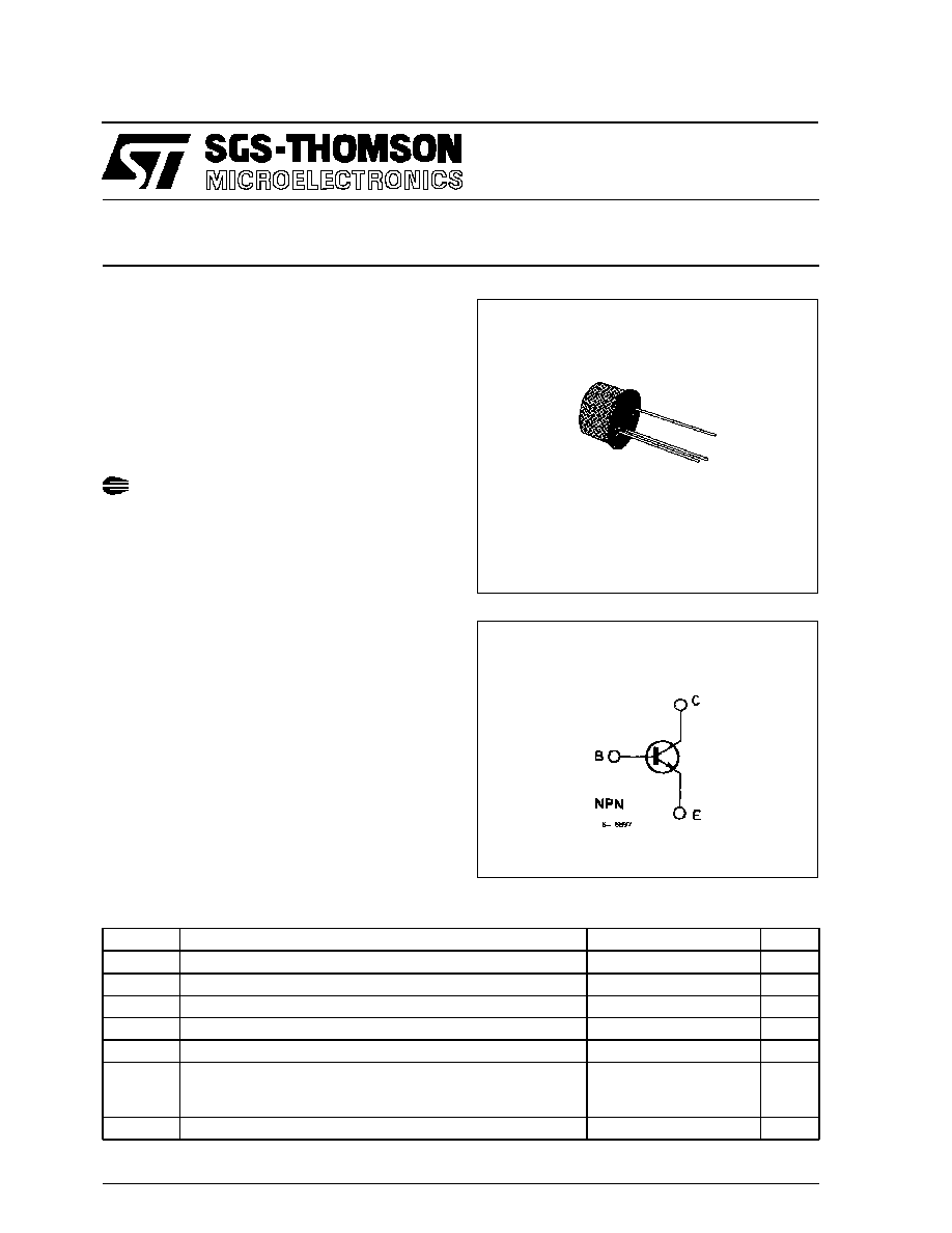
The 2N1893 is a silicon planar epitaxial NPN tran-
sistor in Jedec TO-39 metal case, designed for use
in high-performance amplifier, oscillator and switch-
ing circuits.
It provides greater voltage swings in oscillator and
amplifier circuits and more protection in inductive
switching circuits due to its 120 V collector-to-base
voltage rating.
ABSOLUTE MAXIMUM RATINGS
Symbol
Parameter
Val ue
Unit
V
CBO
Collector-base Voltage (I
E
= 0)
120
V
V
CER
Collector-emitter Voltage (R
BE
10
)
100
V
V
CEO
Collector-emitter Voltage (I
B
= 0)
80
V
V
EBO
Emitter-base Voltage (I
C
= 0)
7
V
I
C
Collector Current
0.5
A
P
t o t
Total Power Dissipation at T
amb
25
∞
C
at T
c as e
25
∞
C
at T
c as e
100
∞
C
0.8
3
1.7
W
W
W
T
s t g
, T
j
Storage and Junction Temperature
≠ 65 to 200
∞
C
INTERNAL SCHEMATIC DIAGRAM
Products approved to CECC 50002-104 avail-
able on request.
DESCRIPTION
TO-39
1/5

ELECTRICAL CHARACTERISTICS (T
amb
= 25
∞
C unless otherwise specified)
Symbol
Parameter
Test Conditions
Min.
Typ.
Max.
Unit
I
CBO
Collector Cutoff Current
(I
E
= 0)
V
CB
= 90 V
V
CB
= 90 V
T
am b
= 150
∞
C
10
15
nA
µ
A
I
E BO
Emitter Cutoff Current
(I
C
= 0)
V
E B
= 5 V
10
nA
V
( BR) CBO
Collector-base Breakdown
Voltage (I
E
= 0)
I
C
= 100
µ
A
120
V
V
(BR)CE R
*
Collector-emitter Breakdown
Voltage (R
BE
10
)
I
C
= 10 mA
100
V
V
(B R)CEO
Collector-emitter Breakdown
Voltage (I
B
= 0)
I
C
= 10 mA
80
V
V
( BR) EBO
Emitter-base Breakdown
Voltage (I
C
= 0)
I
E
= 100
µ
A
7
V
V
CE (s at )
*
Collector-emitter Saturation
Voltage
I
C
= 50 mA
I
C
= 150 mA
I
B
= 5 mA
I
B
= 15 mA
1.2
5
V
V
V
BE (s at )
*
Base-emitter Saturation
Voltage
I
C
= 50 mA
I
C
= 150 mA
I
B
= 5 mA
I
B
= 15 mA
0.82
0.96
0.9
1.3
V
V
h
F E
*
DC Current Gain
I
C
= 0.1 mA
I
C
= 10 mA
I
C
= 150 mA
I
C
= 10 mA
T
amb
= ≠ 55
∞
C
V
CE
= 10 V
V
CE
= 10 V
V
CE
= 10 V
V
CE
= 10 V
20
35
40
20
50
80
80
40
120
h
f e
Small Signal Current Gain
I
C
= 1 mA
f = 1 kHz
I
C
= 5 mA
f = 1 kHz
V
CE
= 5 V
V
CE
= 10 V
30
45
70
85
150
f
T
Transition Frequency
I
C
= 50 mA
f = 20 MHz
V
CE
= 10 V
50
70
MHz
C
EBO
Emitter-base Capacitance
I
C
= 0
f = 1 MHz
V
EB
= 0.5 V
55
85
pF
C
CBO
Collector-base Capacitance
I
E
= 0
f = 1 MHz
V
CB
= 10 V
13
15
pF
* Pulsed : pulse duration = 300
µ
s, duty cycle = 1 %.
THERMAL DATA
R
t h j- cas e
R
t h j-amb
Thermal Resistance Junction-case
Thermal Resistance Junction-ambient
Max
Max
58
219
∞
C/W
∞
C/W
2N1893
2/5

DC Current Gain.
High-frequency Current Gain.
2N1893
3/5
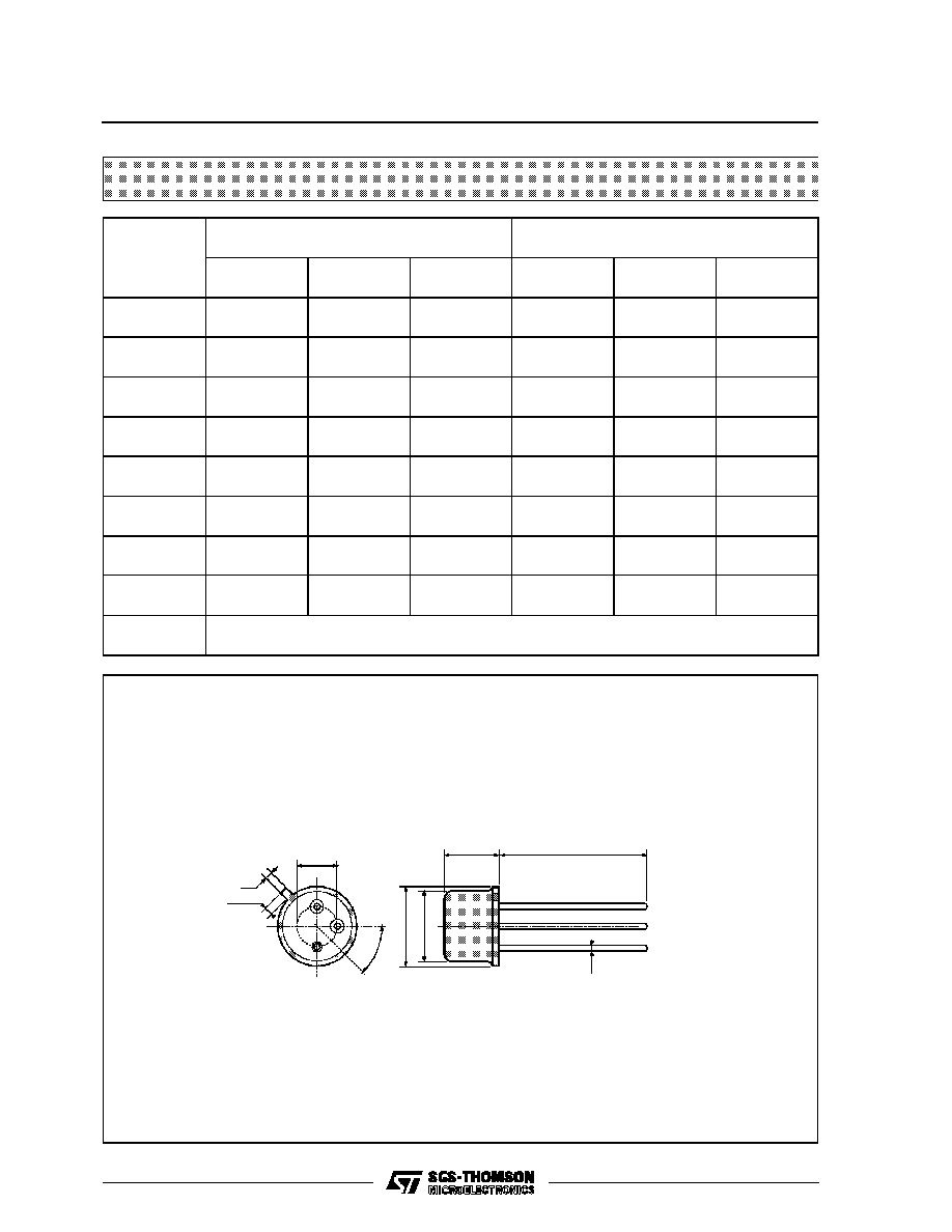
DIM.
mm
inch
MIN.
TYP.
MAX.
MIN.
TYP.
MAX.
A
12.7
0.500
B
0.49
0.019
D
6.6
0.260
E
8.5
0.334
F
9.4
0.370
G
5.08
0.200
H
1.2
0.047
I
0.9
0.035
L
45
o
(typ.)
L
G
I
D
A
F
E
B
H
TO39 MECHANICAL DATA
P008B
2N1893
4/5

Information furnished is believed to be accurate and reliable. However, SGS-THOMSON Microelectronics assumes no responsability for the
consequences of use of such information nor for any infringement of patents or other rights of third parties which may results from its use. No
license is granted by implication or otherwise under any patent or patent rights of SGS-THOMSON Microelectronics. Specifications mentioned
in this publication are subject to change without notice. This publication supersedes and replaces all information previously supplied.
SGS-THOMSON Microelectronics products are not authorized for use as critical components in life support devices or systems without express
written approval of SGS-THOMSON Microelectonics.
©
1994 SGS-THOMSON Microelectronics - All Rights Reserved
SGS-THOMSON Microelectronics GROUP OF COMPANIES
Australia - Brazil - France - Germany - Hong Kong - Italy - Japan - Korea - Malaysia - Malta - Morocco - The Netherlands -
Singapore - Spain - Sweden - Switzerland - Taiwan - Thailand - United Kingdom - U.S.A
2N1893
5/5