2N2219A
2N2222A
HIGH SPEED SWITCHES
DESCRIPTION
The 2N2219A and 2N2222A are silicon planar
epitaxial NPN transistors in Jedec TO-39 (for
2N2219A) and in Jedec TO-18 (for 2N2222A)
metal case. They are designed for high speed
switching application at collector current up to
500mA, and feature useful current gain over a
wide range of collector current, low leakage
currents and low saturation voltage.
Æ
INTERNAL SCHEMATIC DIAGRAM
June 1999
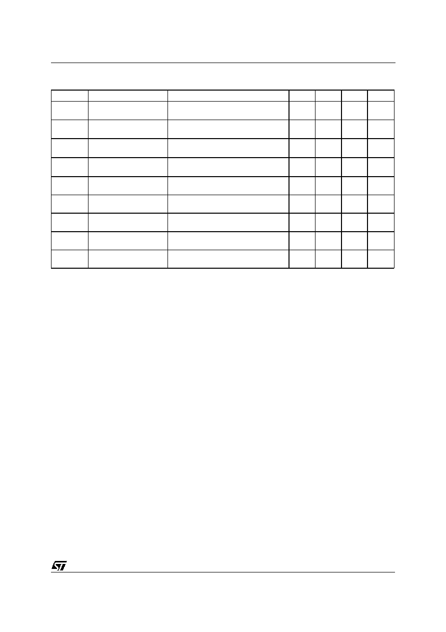
ABSOLUTE MAXIMUM RATINGS
Symb ol
Parameter
Value
Un it
V
CBO
Collector-Base Voltage (I
E
= 0)
75
V
V
CEO
Collector-Emitter Volt age (I
B
= 0)
40
V
V
EBO
Emitter-Base Voltage (I
C
= 0)
6
V
I
C
Collector Current
0.8
A
P
tot
T otal Dissipation at T
amb
25
o
C
for 2N2219A
for 2N2222A
at T
ca se
25
o
C
for 2N2219A
for 2N2222A
0.8
0.5
3
1.8
W
W
W
W
T
s tg
Storage T emperature
-65 to 200
o
C
T
j
Max. Operating Junction Temperat ure
175
o
C
TO-18
TO-39
2N2219A approved to CECC 50002-100,
2N2222A approved to CECC 50002-101
available on request.
1/8

THERMAL DATA
TO-39
T O-18
R
thj -case
R
thj -amb
Thermal Resistance Junction-Case
Max
Thermal Resistance Junction-Ambient
Max
50
187.5
83.3
300
o
C/W
o
C/W
ELECTRICAL CHARACTERISTICS (T
case
= 25
o
C unless otherwise specified)
Symbo l
Parameter
Test Con ditions
Min.
Typ.
Max.
Unit
I
CBO
Collector Cut-of f
Current (I
E
= 0)
V
CB
= 60 V
V
CB
= 60 V
T
case
= 150
o
C
10
10
nA
µ
A
I
CEX
Collector Cut-of f
Current (V
BE
= -3V)
V
CE
= 60 V
10
nA
I
BEX
Base Cut -off Current
(V
BE
= -3V)
V
CE
= 60 V
20
nA
I
EBO
Emitter Cut-of f Current
(I
C
= 0)
V
EB
= 3 V
10
nA
V
(BR) CBO
Collector-Base
Breakdown Voltage
(I
E
= 0)
I
C
= 10
µ
A
75
V
V
(BR) CEO
Collector-Emitt er
Breakdown Voltage
(I
B
= 0)
I
C
= 10 mA
40
V
V
(BR) EBO
Emitter-Base
Breakdown Voltage
(I
C
= 0)
I
E
= 10
µ
A
6
V
V
CE(sat)
Collector-Emitt er
Sat uration Voltage
I
C
= 150 mA
I
B
= 15 mA
I
C
= 500 mA
I
B
= 50 mA
0. 3
1
V
V
V
BE(sat)
Base-Emitter
Sat uration Voltage
I
C
= 150 mA
I
B
= 15 mA
I
C
= 500 mA
I
B
= 50 mA
0. 6
1. 2
2
V
V
h
FE
DC Current G ain
I
C
= 0.1 mA
V
CE
= 10 V
I
C
= 1 mA
V
CE
= 10 V
I
C
= 10 mA
V
CE
= 10 V
I
C
= 150 mA
V
CE
= 10 V
I
C
= 500 mA
V
CE
= 10 V
I
C
= 150 mA
V
CE
= 1 V
I
C
= 10 mA
V
CE
= 10 V
T
amb
= -55
o
C
35
50
75
100
40
50
35
300
h
fe
Small Signal Current
Gain
I
C
= 1 mA
V
CE
= 10 V
f = 1KHz
I
C
= 10 mA
V
CE
= 10 V
f = 1KHz
50
75
300
375
f
T
Transition Frequency
I
C
= 20 mA
V
CE
= 20 V
f = 100 MHz
300
MHz
C
EBO
Emitter Base
Capacitance
I
C
= 0
V
EB
= 0.5 V
f = 100KHz
25
pF
C
CBO
Collector Base
Capacitance
I
E
= 0
V
CB
= 10 V
f = 100 KHz
8
pF
R
e (hie)
Real Part of Input
Impedance
I
C
= 20 mA
V
CE
= 20 V
f = 300MHz
60
Pulsed: Pulse duration = 300
µ
s, duty cycle
1 %
2N2219A/2N2222A
2/8

Contours of Constant Narrow Band Noise Figure.
Switching Time vs. Collector Current.
Normalized DC Current Gain.
Collector-emitter Saturation Voltage.
2N2219A/2N2222A
4/8