 | –≠–ª–µ–∫—Ç—Ä–æ–Ω–Ω—ã–π –∫–æ–º–ø–æ–Ω–µ–Ω—Ç: 2N5321 | –°–∫–∞—á–∞—Ç—å:  PDF PDF  ZIP ZIP |

2N5320
2N5321
SMALL SIGNAL NPN TRANSISTORS
s
SILICON EPITAXIAL PLANAR NPN
TRANSISTORS
s
MEDIUM POWER AMPLIFIER
s
PNP COMPLEMENTS ARE 2N5322 AND
2N5323
DESCRIPTION
The 2N5320 and 2N5321 are silicon epitaxial
planar NPN transistors in Jedec TO-39 metal
case. They are especially intended for
high-voltage medium power application in
industrial and commercial equipments.
The complementary PNP types are respectively
the 2N5322 and 2N5323
INTERNAL SCHEMATIC DIAGRAM
June 1997
TO-39
ABSOLUTE MAXIMUM RATINGS
Symbol
Parameter
Value
Unit
2N5320
2N5321
V
CBO
Collector-Base Voltage (I
E
= 0)
100
75
V
V
CEV
Collector-Emitter Voltage (V
BE
= 1.5V)
100
75
V
V
CEO
Collector-Emitter Voltage (I
B
= 0)
75
50
V
V
EBO
Emitter-Base Voltage (I
C
= 0)
6
5
V
I
C
Collector Current
1.2
A
I
CM
Collector Peak Current
2
A
I
B
Base Current
1
A
P
tot
Total Dissipation at T
amb
= 25
o
C
1
W
P
tot
Total Dissipation at T
c
= 25
o
C
10
W
T
stg
, T
j
Storage and Junction Temperature
-65 to 200
o
C
1/4
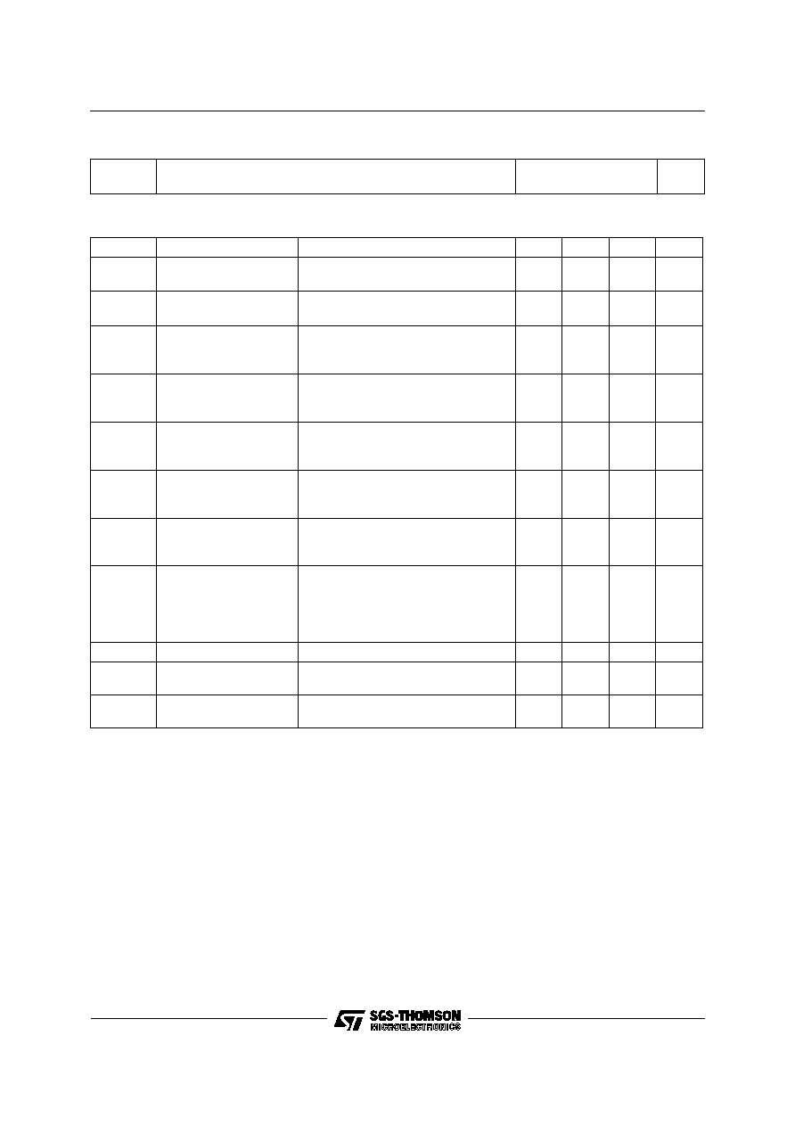
THERMAL DATA
R
thj-case
R
thj-amb
Thermal Resistance Junction-Case Max
Thermal Resistance Junction-Ambient Max
17.5
175
o
C/W
o
C/W
ELECTRICAL CHARACTERISTICS (T
case
= 25
o
C unless otherwise specified)
Symbol
Parameter
Test Conditions
Min.
Typ.
Max.
Unit
I
CBO
Collector Cut-off
Current (I
E
= 0)
V
CB
= 80 V for 2N5320
V
CB
= 60 V for 2N5321
0.5
5
µ
A
µ
A
I
EBO
Collector Cut-off
Current (I
C
= 0)
V
EB
= 5 V for 2N5320
V
EB
= 4 V for 2N5321
0.1
0.5
µ
A
µ
A
V
(BR)CEV
Collector-Emitter
Breakdown Voltage
(V
BE
= 1.5V)
I
C
= 100
µ
A
for 2N5320
for 2N5321
100
75
V
V
V
(BR)CEO
Collector-Emitter
Breakdown Voltage
(I
B
= 0)
I
C
= 10 mA
for 2N5320
for 2N5321
75
50
V
V
V
(BR)EBO
Emitter-Base
Breakdown Voltage
(I
C
= 0)
I
E
= 100
µ
A
for 2N5320
for 2N5321
6
5
V
V
V
CE(sat)
Collector-Emitter
Saturation Voltage
I
C
= 500 mA I
B
= 50 mA
for 2N5320
for 2N5321
0.5
0.8
V
V
V
BE
Base-Emitter Voltage
I
C
= 500 mA V
CE
= 4 V
for 2N5320
for 2N5321
1.1
1.4
V
V
h
FE
DC Current Gain
for 2N5320
I
C
= 500 mA V
CE
= 4 V
I
C
= 1 A V
CE
= 2 V
for 2N5321
I
C
= 500 mA V
CE
= 4 V
30
10
40
130
250
f
T
Transition Frequency
I
C
= 50 mA V
CE
= 4 V f = 10 MHz
50
MHz
t
on
Turn-on Time
I
C
= 500 mA V
CC
= 30 V
I
B1
= 50 mA
80
ns
t
off
Turn-off Time
I
C
= 500 mA V
CC
= 30 V
I
B1
= -I
B2
= 50 mA
800
ns
Pulsed: Pulse duration = 300
µ
s, duty cycle = 1 %
2N5320/2N5321
2/4
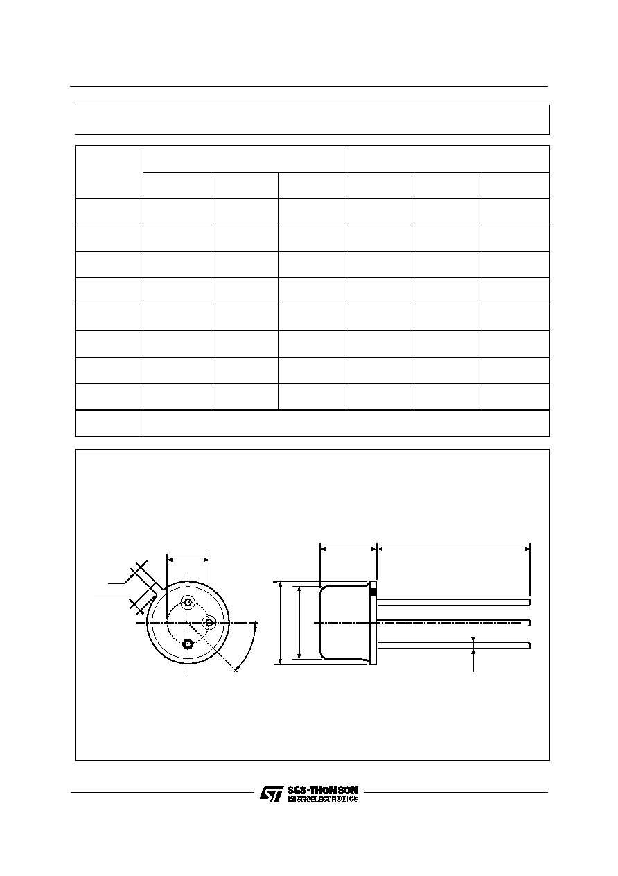
DIM.
mm
inch
MIN.
TYP.
MAX.
MIN.
TYP.
MAX.
A
12.7
0.500
B
0.49
0.019
D
6.6
0.260
E
8.5
0.334
F
9.4
0.370
G
5.08
0.200
H
1.2
0.047
I
0.9
0.035
L
45
o
(typ.)
L
G
I
D
A
F
E
B
H
P008B
TO-39 MECHANICAL DATA
2N5320/2N5321
3/4

Information furnished is believed to be accurate and reliable. However, SGS-THOMSON Microelectronics assumes no responsability for the
consequences of use of such information nor for any infringement of patents or other rights of third parties which may results from its use. No
license is granted by implication or otherwise under any patent or patent rights of SGS-THOMSON Microelectronics. Specifications mentioned
in this publication are subject to change without notice. This publication supersedes and replaces all information previously supplied.
SGS-THOMSON Microelectronics products are not authorized for use as critical components in life support devices or systems without express
written approval of SGS-THOMSON Microelectonics.
© 1997 SGS-THOMSON Microelectronics - Printed in Italy - All Rights Reserved
SGS-THOMSON Microelectronics GROUP OF COMPANIES
Australia - Brazil - Canada - China - France - Germany - Hong Kong - Italy - Japan - Korea - Malaysia - Malta - Morocco - The Netherlands -
Singapore - Spain - Sweden - Switzerland - Taiwan - Thailand - United Kingdom - U.S.A
.
2N5320/2N5321
4/4