November 2005
1/11
11
2STF1360
2STN1360
LOW VOLTAGE FAST-SWITCHING
NPN POWER TRANSISTORS
Features
VERY LOW COLLECTOR-EMITTER
SATUARATION VOLTAGE
HIGH CURRENT GAIN CHARACTERISTIC
FAST-SWITCHING SPEED
IN COMPLANCE WITH THE 2002/93/EC
EUROPEAN DIRECTIVE
SURFACE MOUNTING DEVICES IN MEDIUM
POWER SOT-223 AND SOT-89 PACKAGES
AVAILABLE IN TAPE & REEL PACKING
Applications
EMERGENCY LIGHTING
LED
CCFL DRIVERS (BACK LIGHTING)
VOLTAGE REGULATION
RELAY DRIVER
Description
The 2STF1360 and 2STN1360 are NPN
transistors manufactured using new "PB-HDC"
(Power Bipolar High Density Current) technology.
The resulting transistor shows exceptional high
gain performances coupled with very low
saturation voltage.
Order Codes
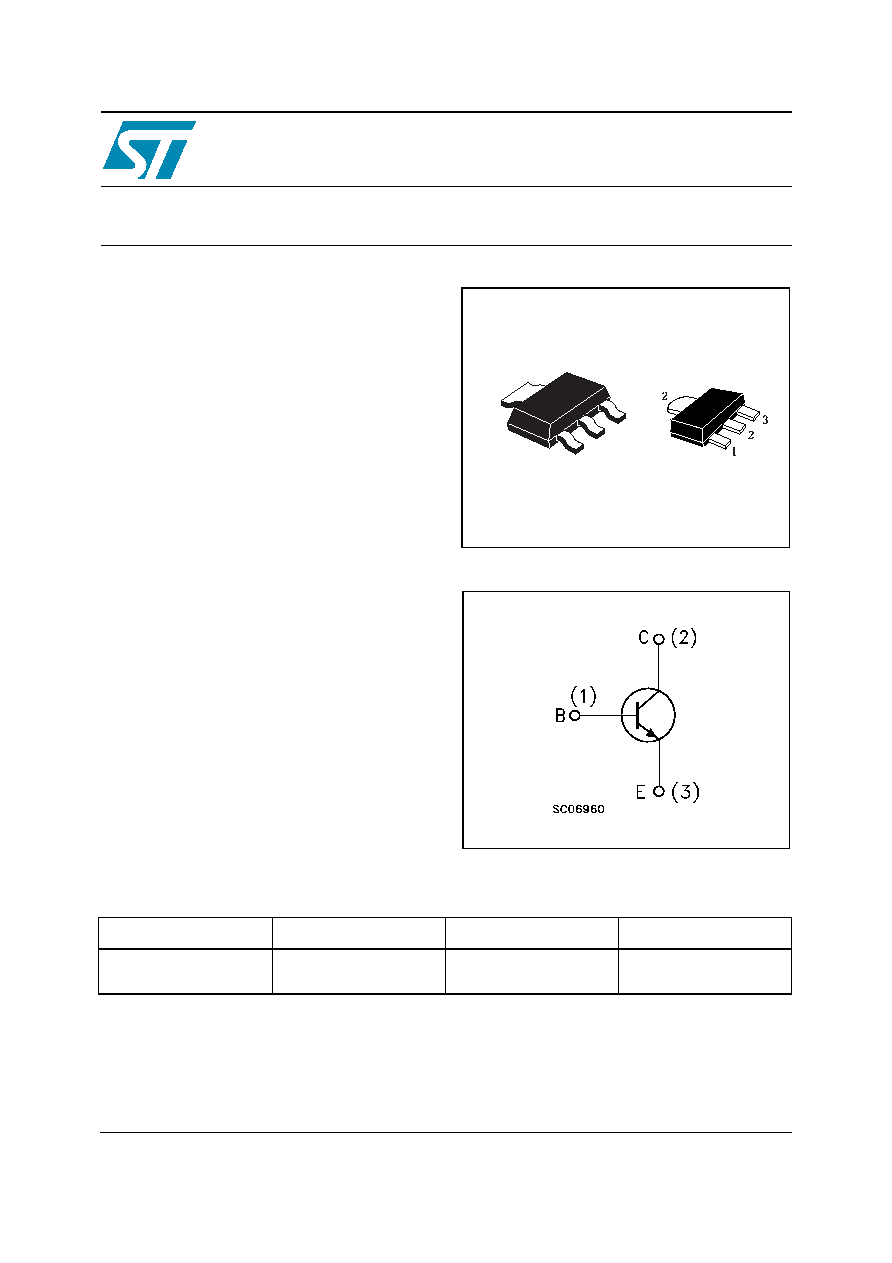
Internal Schematic Diagram
SOT-223 SOT-89
1
2
2
3
Part Number
Marking
Package
Packing
2STF1360
2STN1360
1360
N1360
SOT-89
SOT-223
Tape & Reel
Tape & Reel
www.st.com
rev.1

1 Absolute Maximum Ratings
2STF1360 - 2STN1360
2/11
1 Absolute
Maximum
Ratings
Table 1.
Absolute Maximum Rating
Table 2.
Thermal Data
Note:
# Device mounted on a PCB area of 1 cm
2
.
Symbol
Parameter
Value
Unit
2STF1360
2STN1360
SOT-89
SOT-223
V
CBO
Collector-Base Voltage (I
E
= 0)
80
V
V
CEO
Collector-Emitter Voltage (I
B
= 0)
60
V
V
EBO
Emitter-Base Voltage (I
C
= 0)
6
V
I
C
Collector Current
3
A
I
CM
Collector Peak Current (t
P
< 5ms)
5
A
I
B
Base Current
0.2
A
I
BM
Base Peak Current (t
P
< 5ms)
0.4
A
P
TOT
Total dissipation at T
c
= 25�C
1.4
1.6
W
T
stg
Storage Temperature
-65 to 150
�C
T
J
Max. Operating Junction Temperature
150
�C
Symbol
Parameter
SOT-89
SOT-223
R
thJ-amb
#
Thermal Resistance Junction-Ambient
______ ______
Max
89
78
�C/W

2STF1360 - 2STN1360
2 Electrical Characteristics
3/11
2 Electrical
Characteristics
Table 3.
Electrical Characteristics (T
CASE
= 25�C; unless otherwise specified)
Note: 1 Pulsed duration = 300
�
s, duty cycle
1.5%.
Symbol
Parameter
Test Conditions
Min.
Typ.
Max.
Unit
I
CBO
Collector Cut-off Current
(I
E
= 0)
V
CB
= 80 V
100
nA
I
EBO
Emitter Cut-off Current
(I
C
= 0)
V
EB
= 6 V
100
nA
V
BE
Base-Emitter Voltage
V
CE
= 2 V I
C
= 100 mA
630
670
730
mV
V
CE(sat)
Note: 1
Collector-Emitter Saturation
Voltage
I
C
= 2 A
__ _
I
B
= 100 mA
I
C
= 3 A
__ _
I
B
= 150 mA
150
210
300
500
mV
mV
V
BE(sat)
Note: 1
Base-Emitter Saturation
Voltage
I
C
= 2 A
__ _
I
B
= 100 mA
0.89
1.2
V
h
FE
Note: 1
DC Current Gain
I
C
= 100 mA
_
V
CE
= 2 V
I
C
= 1 A
_
V
CE
= 2 V
80
160
280
400
t
d
t
r
t
s
t
f
RESISTIVE LOAD
Delay Time
Rise Time
Storage Time
Fall Time
V
CC
= 10 V I
C
= 3 A
I
B1
= -
I
B2
= 300 mA
(see figure 8)
17
81
620
54
20
100
720
65
ns
ns
ns
ns
f
T
Transition Frequency
I
C
= 0.1 A
___
V
CE
= 10 V
130
MHz

2 Electrical Characteristics
2STF1360 - 2STN1360
4/11
2.1 Typical
Characteristics
Figure 1.
DC Current Gain
Figure 2.
DC Current Gain
Figure 3.
Collector Emitter Saturation Voltage Figure 4.
Base Emitter Saturation Voltage
Figure 5.
Resistive Load Switching Times
Figure 6.
Resistive LoadSwitching Times

2STF1360 - 2STN1360
2 Electrical Characteristics
5/11
Figure 7.
Reverse Bised SOA