 | –≠–ª–µ–∫—Ç—Ä–æ–Ω–Ω—ã–π –∫–æ–º–ø–æ–Ω–µ–Ω—Ç: 4030B | –°–∫–∞—á–∞—Ç—å:  PDF PDF  ZIP ZIP |
HCC/HCF4030B
November 1996
QUAD EXCLUSIVE-OR GATE
DESCRIPTION
.
MEDIUM-SPEED OPERATION ≠ t
PHL
= t
PLH
=
60ns (typ.) @ C
L
= 50pF and V
DD
≠ V
SS
= 10V
.
LOW OUTPUT IMPEDANCE : 500
(typ.) @
V
DD
≠ V
SS
= 10V
.
QUIESCENT CURRENT SPECIFIED TO 20V
FOR HCC DEVICE
.
STANDARDIZED
SYMMETRICAL
OUTPUT
CHARACTERISTICS
.
5V, 10V, AND 15V PARAMETRIC RATINGS
.
INPUT CURRENT OF 100nA AT 18V AND 25
∞
C
FOR HCC DEVICE
.
100% TESTED FOR QUIESCENT CURRENT
.
MEETS ALL REQUIREMENTS OF JEDEC TEN-
TATIVE STANDARD N
∞
13A, "STANDARD SPE-
CIFICATIONS FOR DESCRIPTION OF "B"
SERIES CMOS DEVICES"
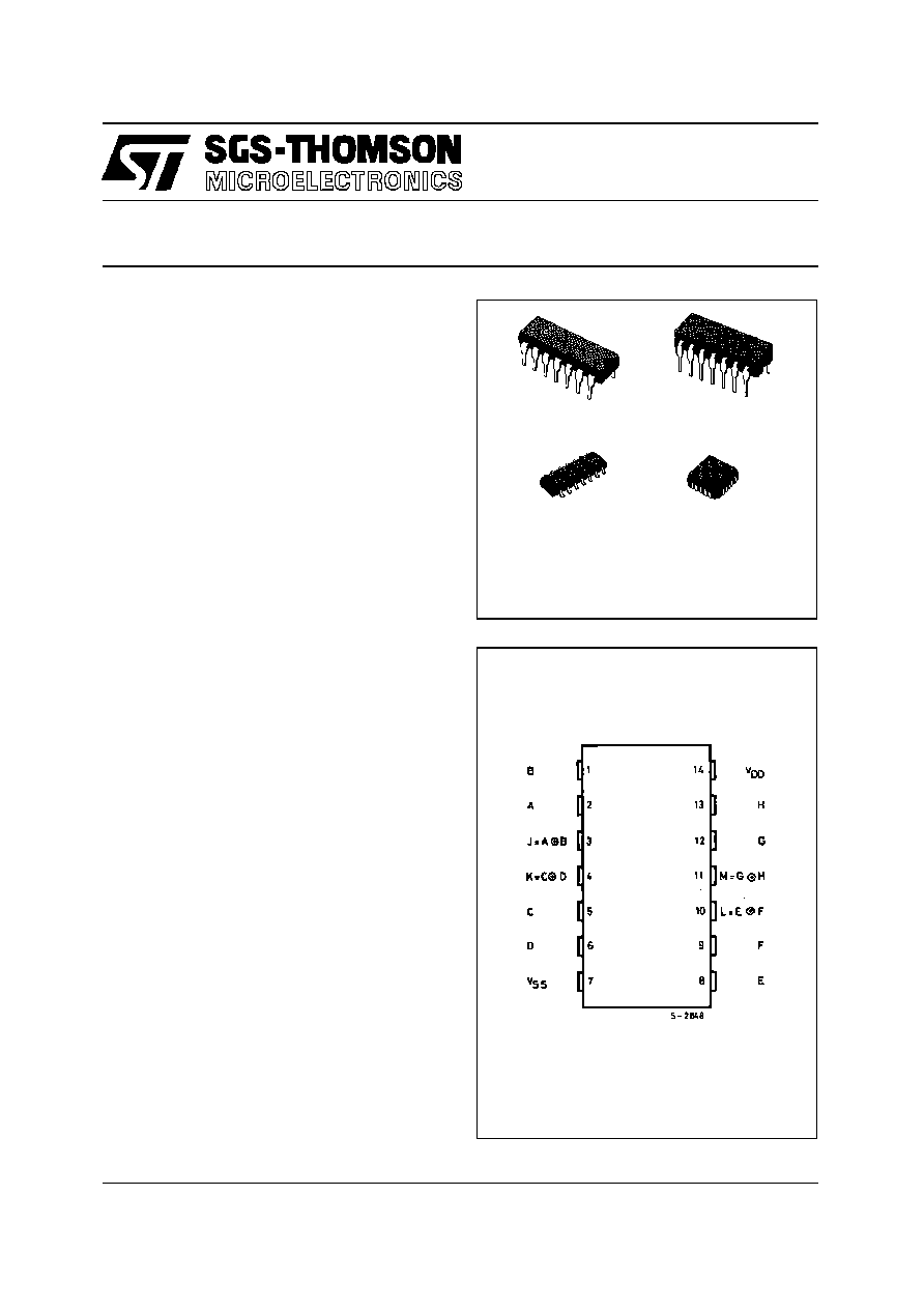
The HCC4030B (extended temperature range) and
HCF4030B (intermediate temperature range) are
monolithic integrated circuit, available in 14-lead
dual in-line plastic or ceramic package and plastic
micro package.
The HCC/HCF4030B types consist of four inde-
pendent exclusive-OR gates integrated on a single
monolithic silicon chip. Each exclusive-OR gate con-
sists of four n-channel and four p-channel enhance-
ment-type transistors. All inputs and outputs are
protected against electrostatic effects.
EY
(Plastic Package)
F
(Ceramic Frit Seal Package)
M1
(Micro Package)
C1
(Plastic Chip Carrier)
ORDER CODES :
HCC4030BF
HCF4030BM1
HCF4030BEY
HCF4030BC1
PIN CONNECTIONS
1/12
ABSOLUTE MAXIMUM RATINGS
Symbol
Parameter
Value
Unit
V
DD
*
Supply Voltage : HCC Types
HCF Types
≠ 0.5 to + 20
≠ 0.5 to + 18
V
V
V
i
Input Voltage
≠ 0.5 to V
DD
+ 0.5
V
I
I
DC Input Current (any one input)
±
10
mA
P
tot
Total Power Dissipation (per package)
Dissipation per Output Transistor
for T
op
= Full Package-temperature Range
200
100
mW
mW
T
op
Operating Temperature : HCC Types
HCF Types
≠ 55 to + 125
≠ 40 to + 85
∞
C
∞
C
T
s tg
Storage Temperature
≠ 65 to + 150
∞
C
Stresses above those listed under "Absolute Maximum Ratings" may cause permanent damage to the device. This is a stress
rating only and functional operation of the device at these or any other conditions above those indicated in the operational sec-
tions of this specifi cation is not implied. Exposure to absolute maximum rating conditions for external periods may affect device
reliability.
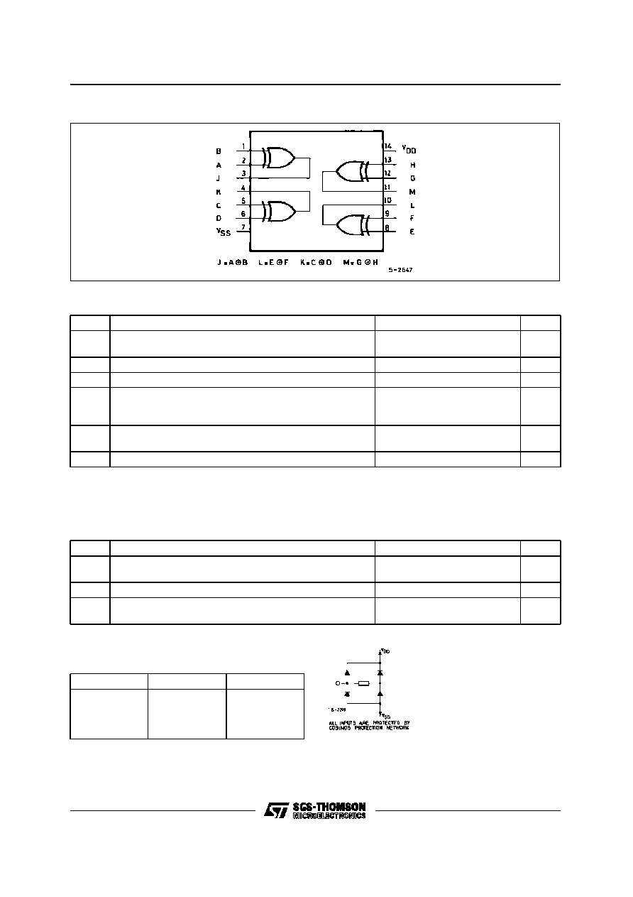
FUNCTIONAL DIAGRAM
TRUTH TABLE
One of Four Identical Gates
A
B
J
0
1
0
1
0
0
1
0
0
1
1
0
Where "1" = High level
"0" = Low level.
RECOMMENDED OPERATING CONDITIONS
Symbol
Parameter
Value
Unit
V
DD
Supply Voltage : HCC Types
HC F Types
3 to 18
3 to 15
V
V
V
I
Input Voltage
0 to V
DD
V
T
o p
Operating Temperature : HCC Types
H CF Types
≠ 55 to + 125
≠ 40 to + 85
∞
C
∞
C
HCC/HCF4030B
2/12

STATIC ELECTRICAL CHARACTERISTICS (over recommended operating conditions)
Test Conditions
Value
V
I
V
O
|I
O
|
V
D D
T
L o w
*
25
∞
C
T
Hi g h
*
Symbol
Parameter
(V)
(V)
(
µ
A)
(V)
Min. Max. Min. Typ. Max. Min. Max.
Unit
I
L
Quiescent
Current
HCC
Types
0/ 5
5
1
0.02
1
30
µ
A
0/10
10
2
0.02
2
60
0/15
15
4
0.02
4
120
0/20
20
20
0.04
20
600
HCF
Types
0/ 5
5
4
0.02
4
30
0/10
10
8
0.02
8
60
0/15
15
16
0.02
16
120
V
O H
Output High
Voltage
0/ 5
< 1
5
4.95
4.95
4.95
V
0/10
< 1
10
9.95
9.95
9.95
0/15
< 1
15
14.95
14.95
14.95
V
O L
Output Low
Voltage
5/0
< 1
5
0.05
0.05
0.05
V
10/0
< 1
10
0.05
0.05
0.05
15/0
< 1
15
0.05
0.05
0.05
V
IH
Input High
Voltage
0.5/4.5
< 1
5
3.5
3.5
3.5
V
1/9
< 1
10
7
7
7
1.5/13.5
< 1
15
11
11
11
V
IL
Input Low
Voltage
4.5/0.5
< 1
5
1.5
1.5
1.5
V
9/1
< 1
10
3
3
3
13.5/1.5
< 1
15
4
4
4
I
O H
Output
Drive
Current
HCC
Types
0/ 5
2.5
5
≠ 2
≠ 1.6 ≠ 3.2
≠ 1.15
mA
0/ 5
4.6
5
≠ 0.64
≠ 0.51 ≠ 1
≠ 0.36
0/10
9.5
10
≠ 1.6
≠ 1.3 ≠ 2.6
≠ 0.9
0/15
13.5
15
≠ 4.2
≠ 3.4 ≠ 6.8
≠ 2.4
HCF
Types
0/ 5
2.5
5
≠ 1.53
≠ 1.36 ≠ 3.2
≠ 1.1
0/ 5
4.6
5
≠ 0.52
≠ 0.44 ≠ 1
≠ 0.36
0/10
9.5
10
≠ 1.3
≠ 1.1 ≠ 2.6
≠ 0.9
0/15
13.5
15
≠ 3.6
≠ 3.0 ≠ 6.8
≠ 2.4
I
O L
Output
Sink
Current
HCC
Types
0/ 5
0.4
5
0.64
0.51
1
0.36
mA
0/10
0.5
10
1.6
1.3
2.6
0.9
0/15
1.5
15
4.2
3.4
6.8
2.4
HCF
Types
0/ 5
0.4
5
0.52
0.44
1
0.36
0/10
0.5
10
1.3
1.1
2.6
0.9
0/15
1.5
15
3.6
3.0
6.8
2.4
I
IH
, I
IL
Input
Leakage
Current
HCC
Types
0/18
Any Input
18
±
0.1
±
10
≠ 5
±
0.1
±
1
µ
A
HCF
Types
0/15
15
±
0.3
±
10
≠ 5
±
0.3
±
1
C
I
Input Capacitance
Any Input
5
7.5
pF
*
T
Lo w
= ≠ 55
∞
C for HCC device : ≠ 40
∞
C for HCF device.
*
T
High
= + 125
∞
C for HCC device : + 85
∞
C for HCF device.
The Noise Margin for both "1" and " 0" level is : 1V min. with V
DD
= 5V, 2V min. with V
DD
= 10V, 2.5 V min. with V
DD
= 15V.
HCC/HCF4030B
3/12
DYNAMIC ELECTRICAL CHARACTERISTICS (T
amb
= 25
∞
C, C
L
= 50pF, R
L
= 200k
,
typical temperature coefficient for all V
D D
= 0.3%/
∞
C values, all input rise and fall time = 20ns)
Value
Symbol
Parameter
Test Conditions
V
C C
(V)
Min.
Typ.
Max.
Unit
t
PL H
, t
PHL
Propagation Delay Time
5
140
280
ns
10
65
130
15
50
100
t
T L H
, t
THL
Transition Time
5
100
200
ns
10
50
100
15
40
80
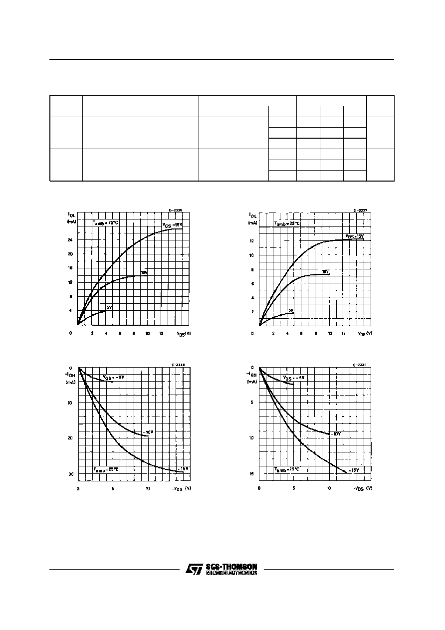
Typical Output Low (sink) Current Characteristics.
Minimum Output Low (sink) Current Charac-
teristics.
Typical Output High (source) Current Charac-
teristics.
Minimum Output High (source) Current Charac-
teristics.
HCC/HCF4030B
4/12
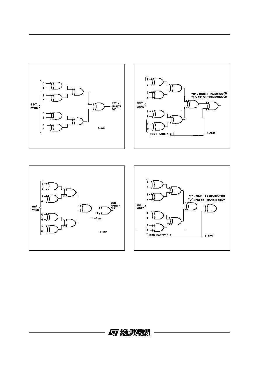
TYPICAL APPLICATIONS
EVEN-PARITY-BIT GENERATOR
(1-3/4 x HCC/HCF4030B).
EVEN-PARITY-CHECKER
(2 x HCC/HCF4030B).
ODD-PARITY-BIT GENERATOR
(2 x HCC/HCF4030B).
ODD-PARITY CHECKER
(2 x HCC/HCF4030B).
HCC/HCF4030B
5/12

8-BIT COMPARATOR
8-BIT TWO'S COMPLEMENT ADDER-SUBSTRACTOR
TYPICAL APPLICATIONS (continued)
HCC/HCF4030B
6/12

The two's complement adder-substractor can add or substract any two of the numbers in table 1. For exam-
ple :
Table 1 : Two's Complement Numbers and Their Equivalent Decimal Values.
a) 2
SIGN
+ =
BIT
≠5 X
0
0
0
0
0
0
1
0
2 +
Y
1
1
1
1
1
0
1
1
≠5 +
CI
0
S 0 1
1
1
1
1
1
0
1 = ≠3
CO
TEST CIRCUITS
Quiescent Device Current.
Input Voltage.
Input Leakage Current.
SIGN
b) ≠2
BIT
≠ = X
1
1
1
1
1
1
1
0 ≠2 +
≠5 Y
1
1
1
1
1
0
1
1 ≠5
Y
0
0
0
0
0
1
0
0
+
CL
1
S 1 0
0
0
0
0
0
1
1
= 3
CO
X8
X7
X6
X5
X4
X3
X2
X1
X8
X7
X6
X5
X4
X3
X2
X1
0
0
0
0
0
0
0
0
=
0
1
1
1
1
1
1
1
1
=
-1
0
0
0
0
0
0
0
1
=
1
1
1
1
1
1
1
1
0
=
-2
0
0
0
0
0
0
1
0
=
2
1
1
1
1
1
1
0
1
=
-3
0
0
0
0
0
0
1
1
=
3
1
1
1
1
1
1
0
0
=
-4
1
1
1
1
1
0
1
1
=
-5
0
1
1
1
1
1
1
0
=
126
1
0
0
0
0
0
0
1
=
-127
0
1
1
1
1
1
1
1
=
127
1
0
0
0
0
0
0
0
=
-128
HCC/HCF4030B
7/12

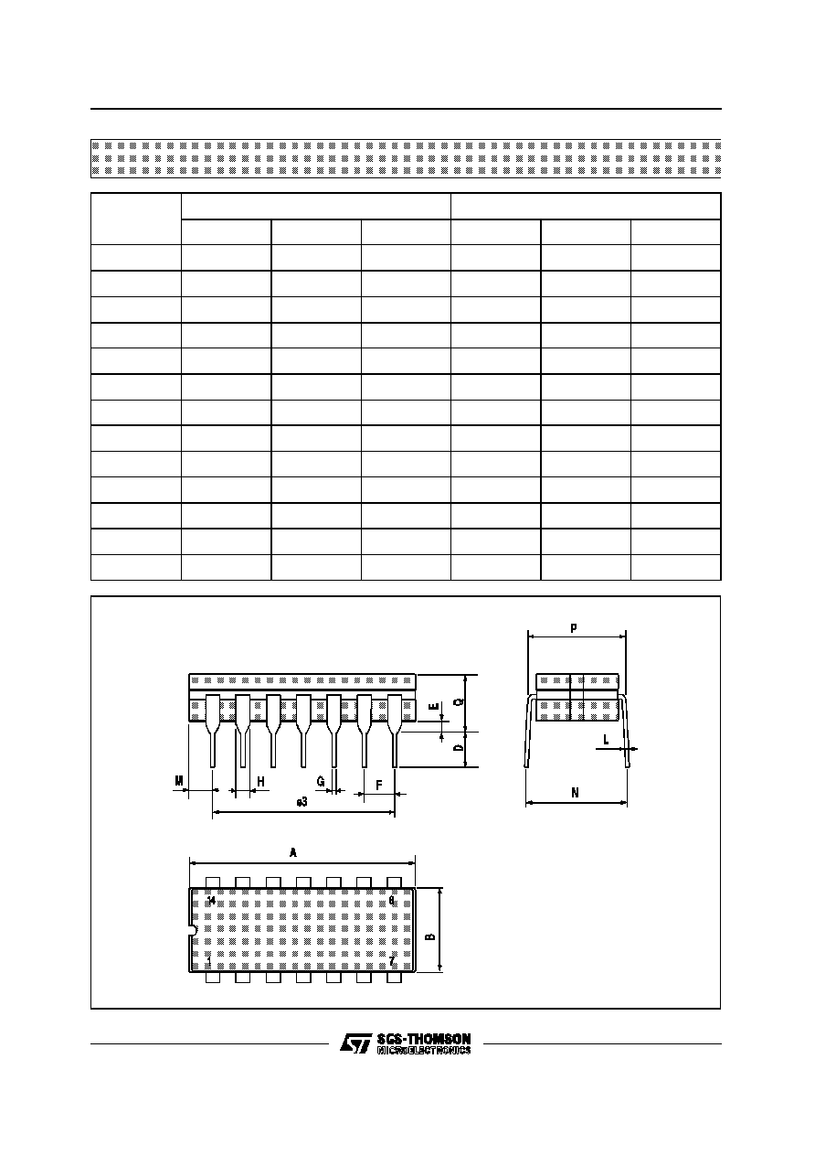
Plastic DIP14 MECHANICAL DATA
DIM.
mm
inch
MIN.
TYP.
MAX.
MIN.
TYP.
MAX.
a1
0.51
0.020
B
1.39
1.65
0.055
0.065
b
0.5
0.020
b1
0.25
0.010
D
20
0.787
E
8.5
0.335
e
2.54
0.100
e3
15.24
0.600
F
7.1
0.280
I
5.1
0.201
L
3.3
0.130
Z
1.27
2.54
0.050
0.100
P001A
HCC/HCF4030B
8/12
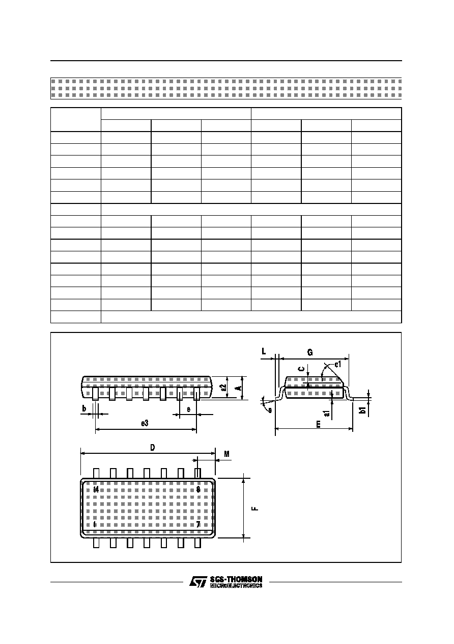
Ceramic DIP14/1 MECHANICAL DATA
DIM.
mm
inch
MIN.
TYP.
MAX.
MIN.
TYP.
MAX.
A
20
0.787
B
7.0
0.276
D
3.3
0.130
E
0.38
0.015
e3
15.24
0.600
F
2.29
2.79
0.090
0.110
G
0.4
0.55
0.016
0.022
H
1.17
1.52
0.046
0.060
L
0.22
0.31
0.009
0.012
M
1.52
2.54
0.060
0.100
N
10.3
0.406
P
7.8
8.05
0.307
0.317
Q
5.08
0.200
P053C
HCC/HCF4030B
9/12
SO14 MECHANICAL DATA
DIM.
mm
inch
MIN.
TYP.
MAX.
MIN.
TYP.
MAX.
A
1.75
0.068
a1
0.1
0.2
0.003
0.007
a2
1.65
0.064
b
0.35
0.46
0.013
0.018
b1
0.19
0.25
0.007
0.010
C
0.5
0.019
c1
45
∞
(typ.)
D
8.55
8.75
0.336
0.344
E
5.8
6.2
0.228
0.244
e
1.27
0.050
e3
7.62
0.300
F
3.8
4.0
0.149
0.157
G
4.6
5.3
0.181
0.208
L
0.5
1.27
0.019
0.050
M
0.68
0.026
S
8
∞
(max.)
P013G
HCC/HCF4030B
10/12
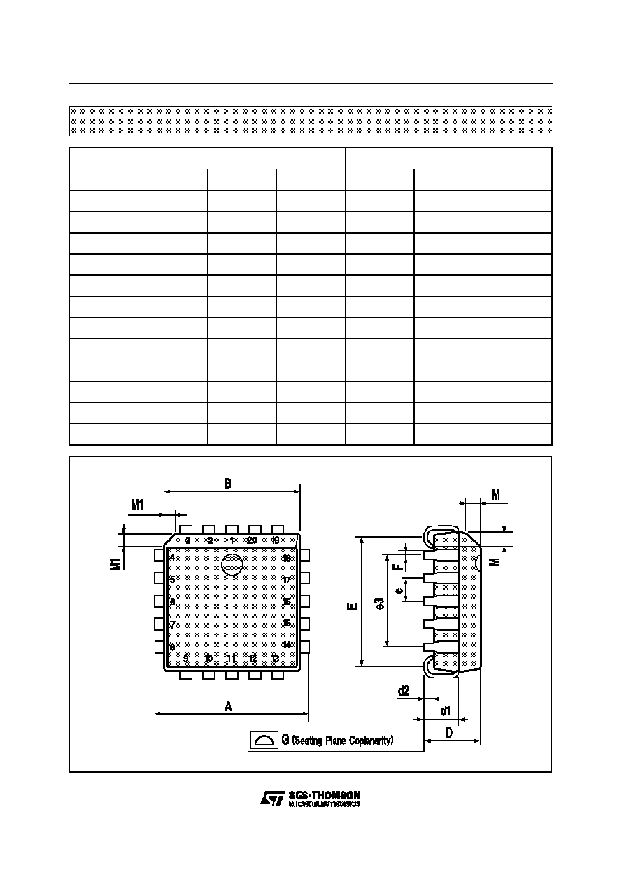
PLCC20 MECHANICAL DATA
DIM.
mm
inch
MIN.
TYP.
MAX.
MIN.
TYP.
MAX.
A
9.78
10.03
0.385
0.395
B
8.89
9.04
0.350
0.356
D
4.2
4.57
0.165
0.180
d1
2.54
0.100
d2
0.56
0.022
E
7.37
8.38
0.290
0.330
e
1.27
0.050
e3
5.08
0.200
F
0.38
0.015
G
0.101
0.004
M
1.27
0.050
M1
1.14
0.045
P027A
HCC/HCF4030B
11/12

Information furnished is believed to be accurate and reliable. However, SGS-THOMSON Microelectronics assumes no responsability for the
consequences of use of such information nor for any infringement of patents or other rights of third parties which may results from its use. No
license is granted by implication or otherwise under any patent or patent rights of SGS-THOMSON Microelectronics. Specifications mentioned
in this publication are subject to change without notice. This publication supersedes and replaces all information previously supplied.
SGS-THOMSON Microelectronics products are not authorized for use as critical components in life support devices or systems without express
written approval of SGS-THOMSON Microelectonics.
©
1996 SGS-THOMSON Microelectronics - Printed in Italy - All Rights Reserved
SGS-THOMSON Microelectronics GROUP OF COMPANIES
Australia - Brazil - Canada - China - France - Germany - Hong Kong - Italy - Japan - Korea - Malaysia - Malta - Morocco - The Netherlands -
Singapore - Spain - Sweden - Switzerland - Taiwan - Thailand - United Kingdom - U.S.A
.
HCC/HCF4030B
12/12