 | –≠–ª–µ–∫—Ç—Ä–æ–Ω–Ω—ã–π –∫–æ–º–ø–æ–Ω–µ–Ω—Ç: 4047B | –°–∫–∞—á–∞—Ç—å:  PDF PDF  ZIP ZIP |

HCC/HCF4047B
June 1989
LOW-POWER MONOSTABLE/ASTABLE MULTIVIBRATOR
.
LOW POWER CONSUMPTION : SPECIAL
COS/MOS OSCILLATOR CONFIGURATION
.
MONOSTABLE (one-shot) OR ASTABLE (free-
running) OPERATION
.
TRUE AND COMPLEMENTED BUFFERED
OUTPUTS
.
ONLY ONE EXTERNAL R AND C REQUIRED
.
BUFFERED INPUTS
.
QUIESCENT CURRENT SPECIFIED TO 20V
FOR HCC DEVICE
.
STANDARDIZED, SYMMETRICAL OUTPUT
CHARACTERISTICS
.
5V, 10V, AND 15V PARAMETRIC RATINGS
.
INPUT CURRENT OF 100nA AT 18V AND 25
∞
C
FOR HCC DEVICE
.
100% TESTED FOR QUIESCENT CURRENT
.
MEETS ALL REQUIREMENTS OF JEDEC TEN-
TATIVE STANDARD N
∞
13A, "STANDARD SPE-
CIFICATIONS FOR DESCRIPTION OF "B"
SERIES CMOS DEVICES"
DESCRIPTION
The HCC4047B (extended temperature range) and
HCF4047B (intermediate temperature range) are
monolithic integrated circuits, available in 14-lead
dual in-line plastic or ceramic package and plas-
tic micropackage. The HCC/HCF4047B consists of
a gatable astable multivibrator with logic techniques
incorporated to permit positive or negative edge-
triggered monostable multivibrator action with retrig-
gering and external counting options. Inputs include
+TRIGGER -TRIGGER, ASTABLE, ASTABLE, RE-
TRIGGER, and EXTERNAL RESET. Buffered out-
puts are Q, Q, and OSCILLATOR. In all modes of
operation, an external capacitor must be connected
between C-Timing and RC-Common terminals, and
an external resistor must be connected between the
R-Timing and RC-Common terminals. For operating
modes see functional terminal connections and ap-
plication notes.
EY
(Plastic Package)
F
(Ceramic Frit Seal Package)
M1
(Micro Package)
C1
(Plastic Chip Carrier)
ORDER CODES :
HCC4047BF
HCF4047BM1
HCF4047BEY
HCF4047BC1
PIN CONNECTIONS
1/15
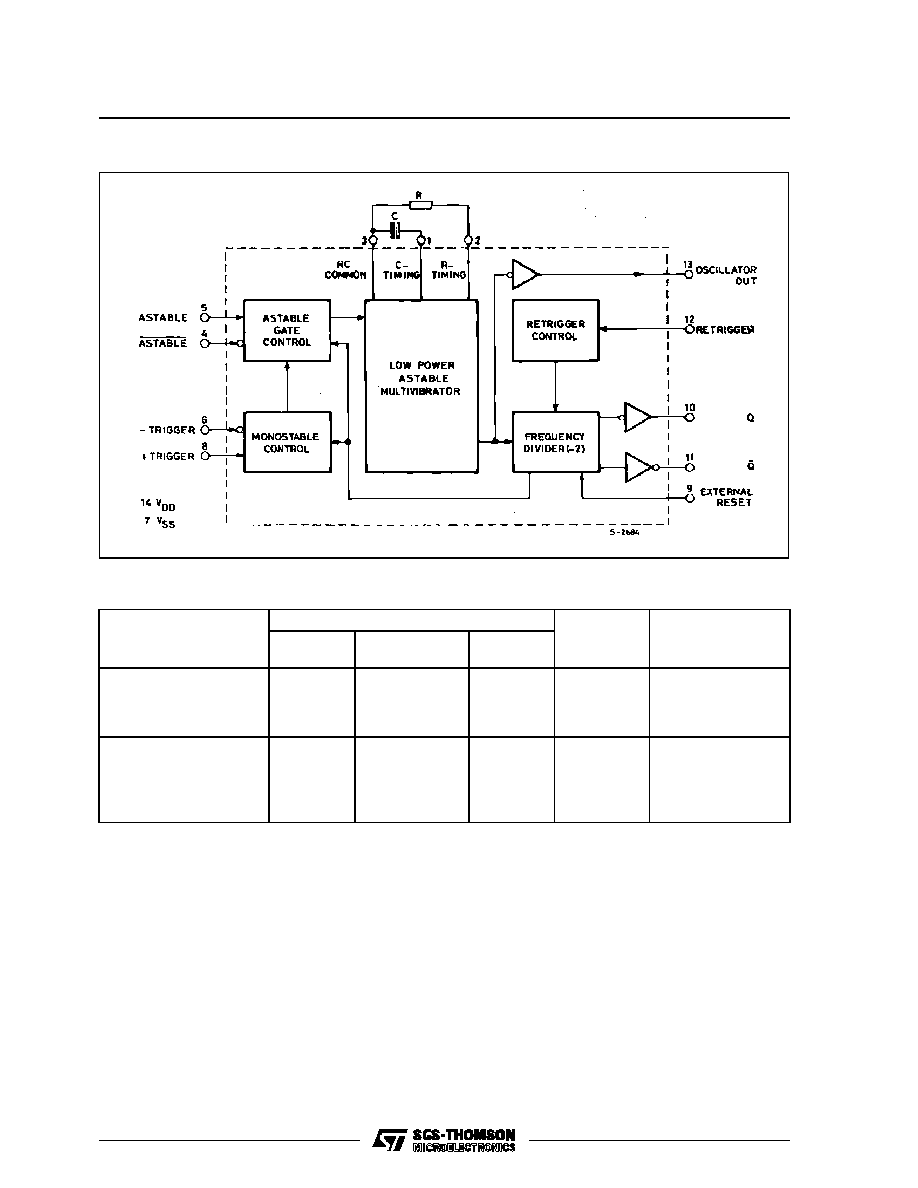
BLOCK DIAGRAM
FUNCTIONAL TERMINAL CONNECTIONS
Terminal Connections
Function*
to V
DD
to V
SS
Input
Pulse to
Output
Pulse
From
Output Period
or
Pulse Width
Astable Multivibrator :
Free Running
True Gating
Complement Gating
4, 5, 6, 14
4, 6, 14
6, 14
7, 8, 9, 12
7, 8, 9, 12
5, 7, 8, 9 ,12
≠
5
4
10, 11, 13
10, 11, 13
10, 11, 13
t
A
(10, 11) = 4.40RC
t
A
(13) = 2.20RC
Monostable Multivibrator :
Positive≠Edge Trigger
Negative≠Edge Trigger
Retriggerable
External Countdown**
4, 14
4, 8, 14
4, 14
14
5, 6, 7, 9, 12
5, 7, 9, 12
5, 6, 7, 9
5, 6, 7, 8, 9, 12
8
6
8, 12
≠
10, 11
10, 11
10, 11
10, 11
t
M
(10, 11) = 2.48RC
* In all cases external capacitor and resistor between pins, 1, 2 and 3 (see logic diagrams).
**
Input pulse to Reset of External Counting Chip.
External Counting Chip Output to pin 4.
HCC/HCF4047B
2/15
ABSOLUTE MAXIMUM RATINGS
Symbol
Parameter
Value
Unit
V
DD
*
Supply Voltage : HCC Types
HCF Types
≠ 0.5 to + 20
≠ 0.5 to + 18
V
V
V
i
Input Voltage
≠ 0.5 to V
DD
+ 0.5
V
I
I
DC Input Current (any one input)
±
10
mA
P
tot
Total Power Dissipation (per package)
Dissipation per Output Transistor
for T
op
= Full Package-temperature Range
200
100
mW
mW
T
op
Operating Temperature : HCC Types
HCF Types
≠ 55 to + 125
≠ 40 to + 85
∞
C
∞
C
T
s tg
Storage Temperature
≠ 65 to + 150
∞
C
Stresses above those listed under "Absolute Maximum Ratings" may cause permanent damage to the device. This is a stress
rating only and functional operation of the device at these or any other conditions above those indicated in the operational sections
of this specification is not implied. Exposure to absolute maximum rating conditions for external periods may affect device reliability.
* All voltage values are referred to V
SS
pin voltage.
RECOMMENDED OPERATING CONDITIONS
Symbol
Parameter
Value
Unit
V
DD
Supply Voltage : HC C Types
H C F Types
3 to 18
3 to 15
V
V
V
I
Input Voltage
0 to V
DD
V
T
o p
Operating Temperature : H CC Types
H C F Types
≠ 55 to + 125
≠ 40 to + 85
∞
C
∞
C
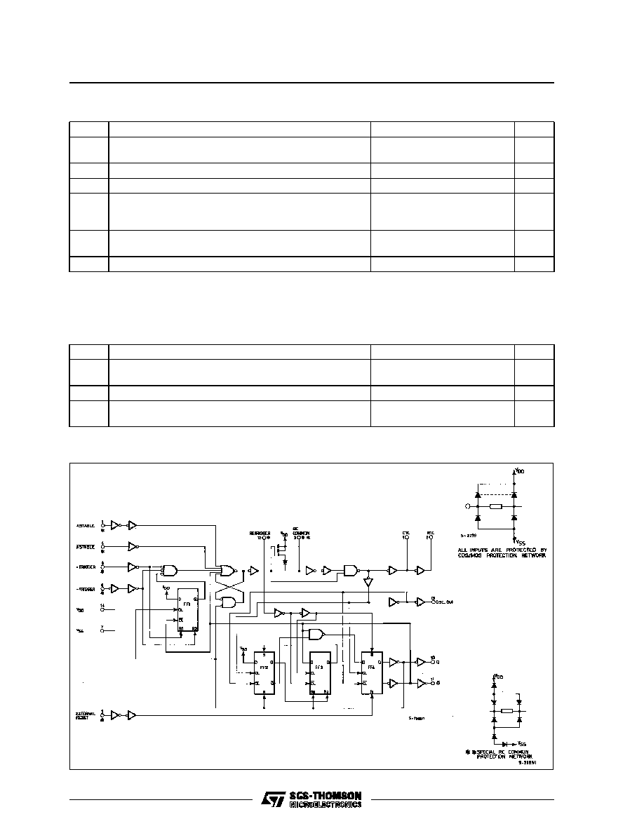
LOGIC DIAGRAM
HCC/HCF4047B
3/15

Detail for Flip-flops FF1 and FF3 (a) and for Flip-flops FF2 and FF4 (b).
STATIC ELECTRICAL CHARACTERISTICS (over recommended operating conditions)
Test Conditions
Value
V
I
V
O
|I
O
|
V
DD
T
Low
*
25
∞
C
T
Hi gh
*
Symbol
Parameter
(V)
(V)
(
µ
A)
(V)
Min.
Max.
Min.
Typ. Max.
Min.
Max.
Unit
I
L
Quiescent
Current
HCC
Types
0/ 5
5
1
0.02
1
30
µ
A
0/10
10
2
0.02
2
60
0/15
15
4
0.02
4
120
0/20
20
20
0.04
20
600
HCF
Types
0/ 5
5
4
0.02
4
30
0/10
10
8
0.02
8
60
0/15
15
16
0.02
16
120
V
OH
Output High
Voltage
0/ 5
< 1
5
4.95
4.95
4.95
V
0/10
< 1
10
9.95
9.95
9.95
0/15
< 1
15
14.95
14.95
14.95
V
OL
Output Low
Voltage
5/0
< 1
5
0.05
0.05
0.05
V
10/0
< 1
10
0.05
0.05
0.05
15/0
< 1
15
0.05
0.05
0.05
V
IH
Input High
Voltage
0.5/4.5
< 1
5
3.5
3.5
3.5
V
1/9
< 1
10
7
7
7
1.5/13.5
< 1
15
11
11
11
* T
Lo w
= ≠ 55
∞
C for HCC device : ≠ 40
∞
C for HCF device.
* T
High
= + 125
∞
C for HCC device : + 85
∞
C for HCF device.
The Noise Margin for both "1" and " 0" level is : 1V min. with V
DD
= 5V, 2V min. with V
DD
= 10V, 2.5V min. with V
DD
= 15V.
HCC/HCF4047B
4/15

DYNAMIC ELECTRICAL CHARACTERISTICS (T
amb
= 25
∞
C, C
L
= 50pF, R
L
= 200k
,
typical temperature coefficient for all V
DD
values is 0.3%/
∞
C, all input rise and fall times = 20ns)
Value
Symbol
Parameter
Test Conditions
V
DD
(V)
Min.
Typ.
Max.
Unit
t
PLH
, t
PHL
Propagation
Delay Time
Astable, Astable to
osc. out
5
200
400
ns
10
100
200
15
80
160
Astable, Astable to
Q, Q
5
350
700
10
175
350
15
125
250
+ or ≠ Trigger to
Q, Q
5
500
1000
10
225
450
15
150
300
STATIC ELECTRICAL CHARACTERISTICS (continued)
Test Conditions
Value
V
I
V
O
|I
O
|
V
DD
T
Low
*
25
∞
C
T
Hi gh
*
Symbol
Parameter
(V)
(V)
(
µ
A)
(V)
Min.
Max.
Min.
Typ. Max.
Min.
Max.
Unit
V
IL
Input Low
Voltage
4.5/0.5
< 1
5
1.5
1.5
1.5
V
9/1
< 1
10
3
3
3
13.5/1.5
< 1
15
4
4
4
I
OH
Output
Drive
Current
HCC
Types
0/ 5
2.5
5
≠ 2
≠ 1.6 ≠ 3.2
≠ 1.15
mA
0/ 5
4.6
5
≠ 0.64
≠ 0.51
≠ 1
≠ 0.36
0/10
9.5
10
≠ 1.6
≠ 1.3 ≠ 2.6
≠ 0.9
0/15
13.5
15
≠ 4.2
≠ 3.4 ≠ 6.8
≠ 2.4
HCF
Types
0/ 5
2.5
5
≠ 1.53
≠ 1.36 ≠ 3.2
≠ 1.1
0/ 5
4.6
5
≠ 0.52
≠ 0.44
≠ 1
≠ 0.36
0/10
9.5
10
≠ 1.3
≠ 1.1 ≠ 2.6
≠ 0.9
0/15
13.5
15
≠ 3.6
≠ 3.0 ≠ 6.8
≠ 2.4
I
OL
Output
Sink
Current
HCC
Types
0/ 5
0.4
5
0.64
0.51
1
0.36
mA
0/10
0.5
10
1.6
1.3
2.6
0.9
0/15
1.5
15
4.2
3.4
6.8
2.4
HCF
Types
0/ 5
0.4
5
0.52
0.44
1
0.36
0/10
0.5
10
1.3
1.1
2.6
0.9
0/15
1.5
15
3.6
3.0
6.8
2.4
I
IH
, I
IL
Input
leakage
Curent
HCC
Types
0/18
Any Input
18
±
0.1
±
10
≠5
±
0.1
±
1
µ
A
HCF
Types
0/15
15
±
0.3
±
10
≠5
±
0.3
±
1
C
I
Input Capacitance
Any Input
5
7.5
pF
* T
Low
= ≠ 55
∞
C for HCC device : ≠ 40
∞
C for HCF device.
* T
High
= + 125
∞
C for HCC device : + 85
∞
C for HCF device.
The Noise Margin for both "1" and "0" level is : 1V min. with V
DD
= 5V, 2V min. with V
DD
= 10V, 2.5V min. with V
DD
= 15V.
HCC/HCF4047B
5/15