 | –≠–ª–µ–∫—Ç—Ä–æ–Ω–Ω—ã–π –∫–æ–º–ø–æ–Ω–µ–Ω—Ç: 405 | –°–∫–∞—á–∞—Ç—å:  PDF PDF  ZIP ZIP |
1/7
July, 3 2002
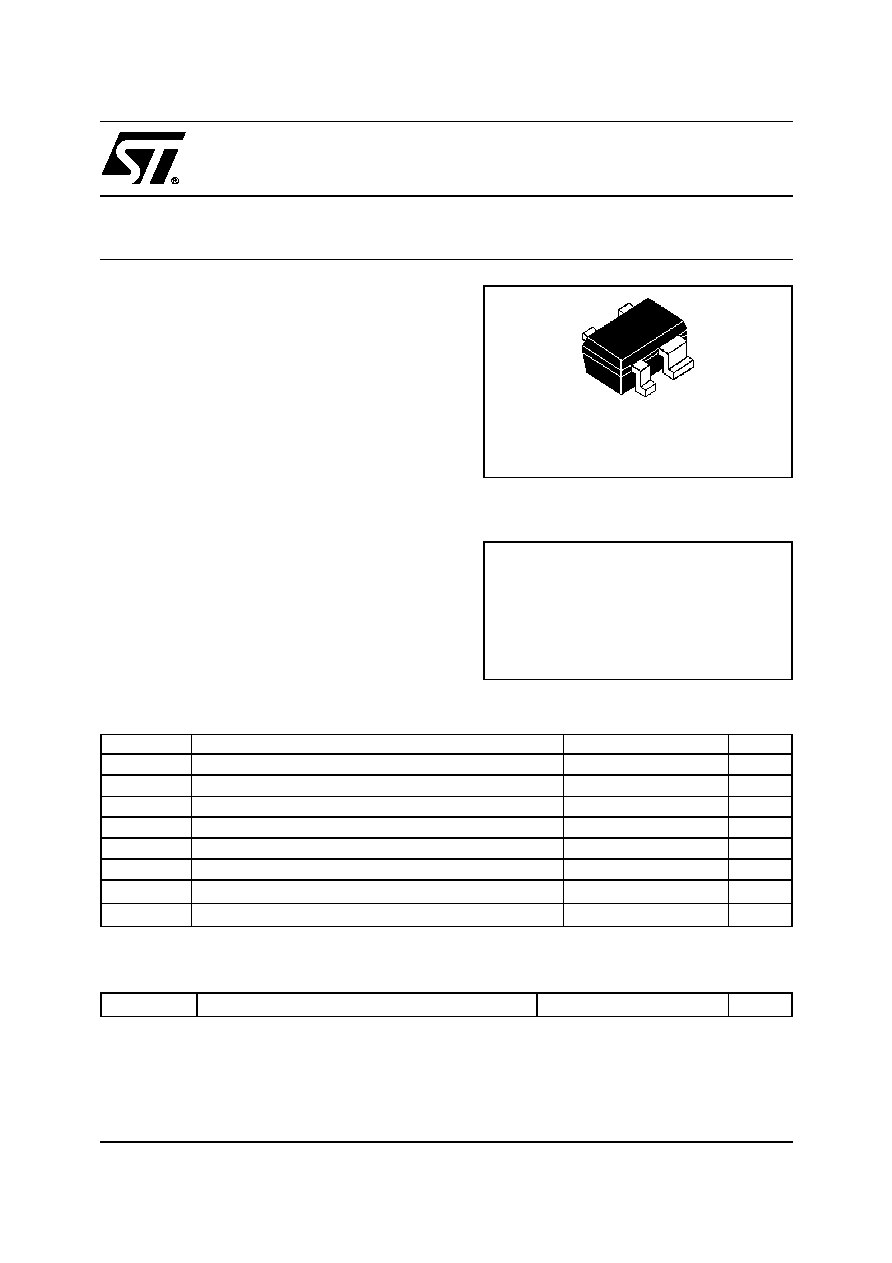
START405
NPN Silicon RF Transistor
SOT343 (SC70)
ORDER CODE
START405TR
BRANDING
405
APPLICATIONS
∑ LNA FOR GSM/DCS, DECT, PCS, PCN,
CDMA, W-CDMA
∑ GENERAL PURPOSE 500MHz-5GHz
∑ LOW NOISE FIGURE: NFmin = 1.1dB
@ 1.8GHz, 2mA, 2V
∑ COMPRESSION P1dB = 5dBm
@ 1.8GHz, 5mA, 2V
∑ TRANSITION FREQUENCY 42GHz
∑ LOW CURRENT CONSUMPTION
∑ ULTRA MINIATURE SOT343 PACKAGE
DESCRIPTION
The START405 is a member of the START family
that provide the state of the art of RF silicon process
to the market. Manufacturated in the third
generation of ST proprietary bipolar process, it
offers the best mix of gain and NF for given
breakdown voltage(BVceo).
It offers performance level only archived with GaAs
products before.
ABSOLUTE MAXIMUM RATINGS
Symbol
Parameter
Value
Unit
V
ceo
Collector emitter voltage
4.5
V
V
cbo
Collector base voltage
15
V
V
ebo
Emitter base voltage
1.5
V
I
c
Collector current
10
mA
I
b
Base current
1
mA
P
tot
Total dissipation, T
s
=
TBD
45
mW
T
stg
Storage temperature
-65 to 150
o
C
T
j
Max. operating junction temperature
150
o
C
R
thjs
Thermal Resistance Junction soldering point
270
o
C/W
ABSOLUTE MAXIMUM RATINGS
START405
2/7
ELECTRICAL CHARACTERISTICS (T
j
=25
o
C,unless otherwise specified)
Note(1): Gms = | S
21
/ S
12
|
Symbol
Parameter
Test Conditions
Min.
Typ.
Max.
Unit
I
cbo
Collector cutoff current
Vcb =5V, Ie = 0A
150
nA
I
ebo
Emitter-base cutoff
current
Veb = 1.5V, Ic = 0A
15
µ
A
Hfe
DC current gain
Ic = 5mA, Vce = 4V
160
NFmin
Minimim noise figure
Ic = 2mA, Vce = 2V, f = 1.8GHz
1.1
dB
Ga
NFmin associated gain
Ic = 2mA, Vce = 2V, f = 1.8GHz
19
dB
|S21|
2
Insertion power gain
Ic = 5mA, Vce = 2V, f = 1.8GHz
17.4
dB
Gms
(1)
Maximum stable gain
Ic = 5mA, Vce = 2V, f = 1.8GHz
24.2
dB
P
-1dB
1dB compression point
Ic = 5mA,Vce = 2V, f = 1.8GHz
5
dBm
OIP3
Ouput third order
intercept point
Ic = 5mA,Vce = 2V, f = 1.8GHz
15
dBm
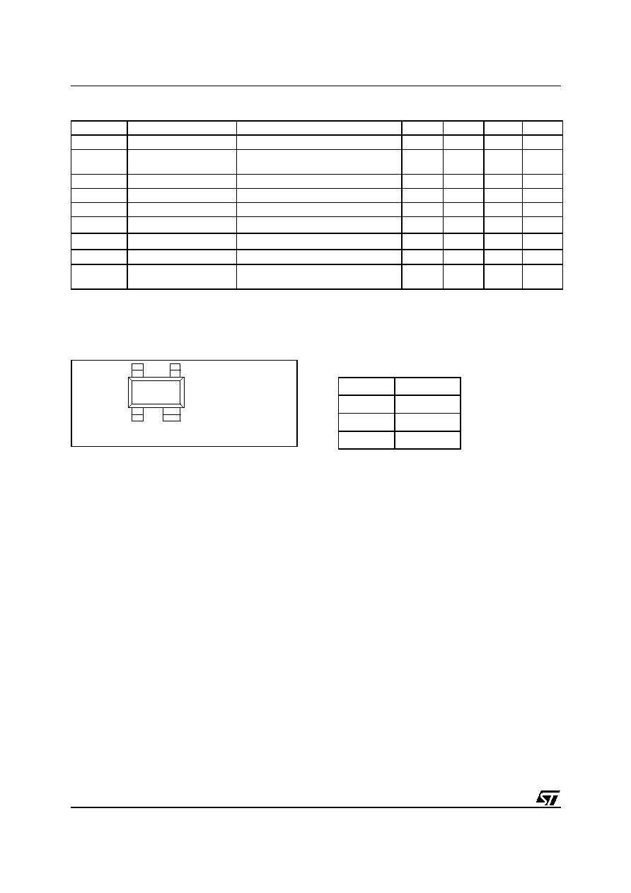
PINOUT
PIN CONNECTION
Pin No.
Description
1
BASE
3
COLLECTOR
2,4
EMITTER
SOT343
4
1
2
3
Top view
3/7
START405
Symbol
Value
Symbol
Value
Symbol
Value
TMEAS
27.0
FC
0.5
XJBC
0.3
IS
1.9E-17
EG
1.12
XTI
3.57
ISE
1.58E-13
NF
1
BF
340
NR
1
NE
2.711
VAF
79
ISC
7.40E-17
BR
8.59
VAR
2.35
IKF
{0.151*((T(
o
C)+273.15)/
300.15)^(-1.774)}
NC
1.312
TF
4.1E-12
TR
7E-10
PTF
38
VTF
14.7
XTF
42
ITF
0.42
MJE
0.414
RB
34.07
RBM
6.1
MJC
0.266
RC
7.9
RE
1.25
MJS
0.22
CJE
111E-15
VJE
1.1
IKR
2.29E-3
CJC
53E-15
VJC
0.69
XTB
-0.744
CJS
33E-15
VJS
0.4
SPICE PARAMETERS (Gummel-Poon Model, Berkley-SPICE 2G.6 Syntax)
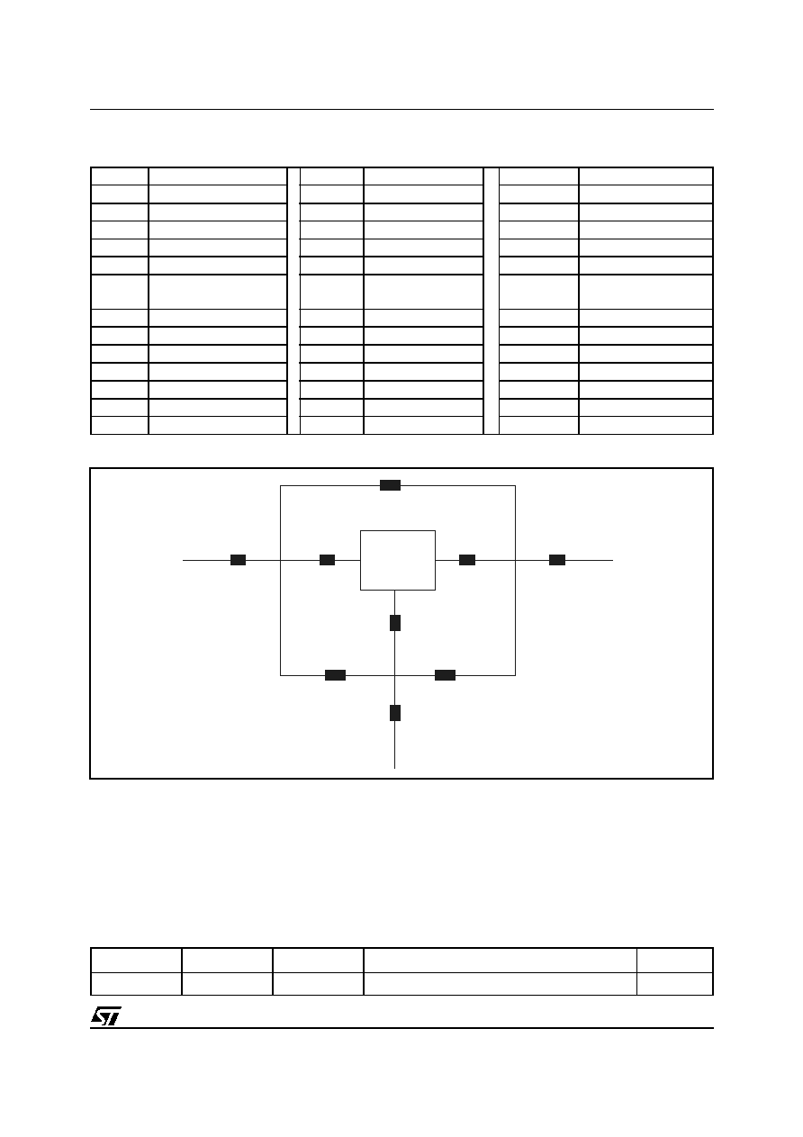
PACKAGE EQUIVALENT CIRCUIT
TRANSISTOR CHIP DATA
FOR MORE ACCURACY SIMULATION IN SATURATION REGION :
Adding the 5 Spice parameters showed in Table A and using ST Spice Library (available on request) you
can achieve a more accuracy simulation in the saturation region. ST Spice library is compatible with
following simulators: ELDO MENTOR (any version), SPECTRE CADENCE (any version), ADS (version
2001 only).
Table A (Spice Parameters extracted in saturation region)
RW
Vjj
ENP
VRP
RP
2.594
0.769
2.045
{8.67*((TEMPER+273.15)/300.15)^(0.839)}
1.00E-6
In order to avoid high complexity of the package equivalent circuit, the two emitter leads of SOT-343
package are combined in one electrical connection.
C
Transistor
Chip
B'
C'
E'
L=0.3 nH
L=0.6 nH
L3
L5
L6
C2
C=5 fF
.
.
L=0.35 nH
L1
L=0.3 nH
L=0.15 nH
L2
C=300 fF
C=430 fF
C1
C3
E
.
.
L=0.6 nH
L4
B
.
.
C
Transistor
Chip
B'
C'
E'
L=0.3 nH
L=0.6 nH
L3
L5
L6
C2
C=5 fF
.
.
L=0.35 nH
L1
L=0.3 nH
L=0.15 nH
L2
C=300 fF
C=430 fF
C1
C3
E
.
.
L=0.6 nH
L4
B
.
.
START405
4/7
COMMON EMITTER S-PARAMETERS ( V
CE
= 2V, I
C
= 5mA )
FREQ
IS
11
I
IS
21
I
IS
12
I
S
12
IS
22
I
S
22
(MHz)
0.1
0.903
-5
12.29
176
0.007
95
0.991
-2
0.5
0.882
-23
10.96
174
0.014
97
0.971
-11
0.9
0.825
-38
9.71
174
0.021
98
0.918
-19
1
0.809
-41
9.42
175
0.022
99
0.906
-20
1.5
0.713
-53
8.11
177
0.027
107
0.850
-24
1.8
0.674
-58
7.43
180
0.028
114
0.829
-27
2
0.642
-61
6.99
178
0.028
122
0.820
-28
2.5
0.579
-64
6.01
172
0.028
148
0.815
-30
3
0.523
-64
5.12
164
0.030
175
0.815
-31
3.5
0.462
-67
4.31
156
0.039
131
0.787
-35
4
0.372
-78
3.48
146
0.065
94
0.644
-41
S
11
S
21

5/7
START405
TAPE & REEL DIMENSIONS
mm
MIN.
TYP.
MAX
A
178.5
179
179.5
C
12.8
13.0
13.5
D
20.2
N
54.5
55
55.5
T
14.4
Ao
2.25
Bo
2.7
Ko
1.2
Po
3.8 (cumulative 10 Po)
4.0
4.2 (cumulative 10 Po)
P
4.0
DEVICE ORIENTATION
TOP
VIEW END
VIEW
405
405
405
405