 | –≠–ª–µ–∫—Ç—Ä–æ–Ω–Ω—ã–π –∫–æ–º–ø–æ–Ω–µ–Ω—Ç: 4066 | –°–∫–∞—á–∞—Ç—å:  PDF PDF  ZIP ZIP |
1/9
September 2001
s
15V DIGITAL OR
±
7.5V PEAK TO PEAK
SWITCHING
s
125
TYPICAL ON RESISTANCE FOR 15V
OPERATION
s
SWITCH ON RESISTANCE MATCHED TO
WITHIN 5
TYP. OVER 15V SIGNAL INPUT
RANGE
s
ON RESISTANCE FLAT OVER FULL PEAK
TO PEAK SIGNAL RANGE
s
HIGH ON/OFF OUTPUT VOLTAGE RATIO :
65dB TYP. at f
IS
= 10KHz, R
L
= 10K
s
HIGH DEGREE OF LINEARITY : < 0.5%
DISTORTION TYP. at f
IS
= 1KHz, V
IS
= 5 V
pp
,
V
DD
- V
SS
> 10V, RL = 10K
s
EXTREMELY LOW OFF SWITCH LEAKAGE
RESULTING IN VERY LOW OFFSET
CURRENT AND HIGH EFFECTIVE OFF
RESISTANCE : 10pA TYP.
at V
DD
- V
SS
= 10V, T
amb
= 25
∞
C
s
EXTREMELY HIGH CONTROL INPUT
IMPEDANCE (control circuit isolated from
signal circuit 10
12
typ.)
s
LOW CROSSTALK BETWEEN SWITCHES :
50dB Typ. at f
IS
= 0.9MHz, R
L
= 1K
s
MATCHED CONTROL - INPUT TO SIGNAL
OUTPUT CAPACITANCE : REDUCES
OUTPUT SIGNAL TRANSIENTS
s
FREQUENCY RESPONSE SWITCH ON :
40MHz (Typ.)
s
QUIESCENT CURRENT SPECIF. UP TO 20V
s
5V, 10V AND 15V PARAMETRIC RATINGS
s
INPUT LEAKAGE CURRENT
I
I
= 100nA (MAX) AT V
DD
= 18V T
A
= 25
∞
C
s
100% TESTED FOR QUIESCENT CURRENT
s
MEETS ALL REQUIREMENTS OF JEDEC
JESD13B " STANDARD SPECIFICATIONS
FOR DESCRIPTION OF B SERIES CMOS
DEVICES"
DESCRIPTION
The HCF4066B is a monolithic integrated circuit
fabricated
in
Metal
Oxide
Semiconductor
technology available in DIP and SOP packages.
The HCF4066B is a QUAD BILATERAL SWITCH
intended for the transmission or multiplexing of
analog or digital signals.
It is pin for pin compatible with HCF4016B, but
exhibits a much lower ON resistance. In addition,
HCF4066B
QUAD BILATERAL SWITCH FOR TRANSMISSION OR
MULTIPLEXING OF ANALOG OR DIGITAL SIGNALS
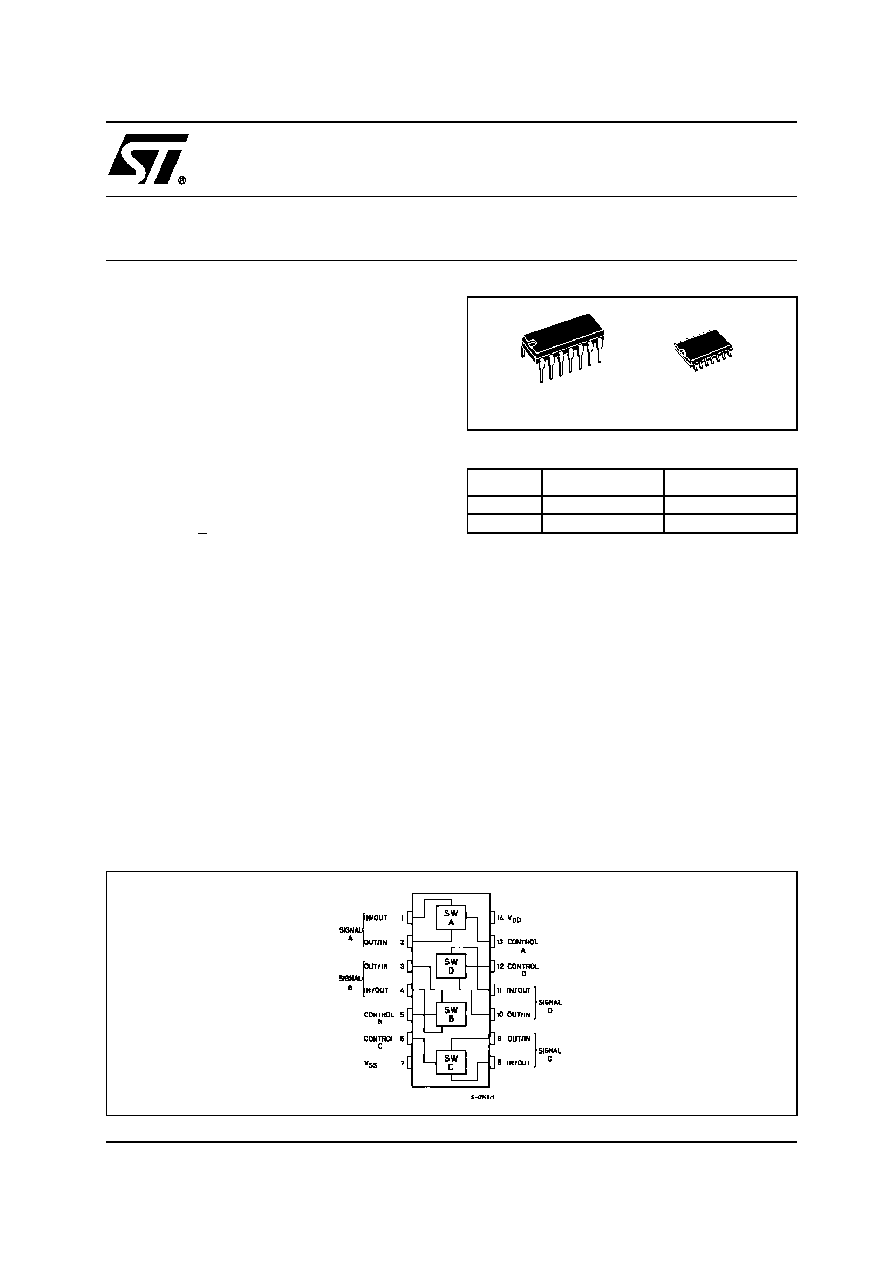
PIN CONNECTION
ORDER CODES
PACKAGE
TUBE
T & R
DIP
HCF4066BEY
SOP
HCF4066BM1
HCF4066M013TR
DIP
SOP

HCF4066B
2/9
the ON resistance is relatively constant over the
full input signal range. The HCF4066B consists of
four independent bilateral switches. A single
control signal is required per switch. Both the p
and n device in a given switch are biased ON or
OFF simultaneously by the control signal. As
shown in schematic diagram , the well of the
n-channel device on each switch is either tied to
the input when the switch is ON or to V
SS
when
the switch is OFF. This configuration eliminates
the variation of the switch-transistor threshold
voltage with input signal, and thus keeps the ON
resistance low over the full operating signal range.
The advantages over single channel switches
include peak input signal voltage swings equal to
the full supply voltage, and more constant ON
impedance over the input signal range. For
sample and hold applications, however, the
HCF4016B is recommended.
INPUT EQUIVALENT CIRCUIT
PIN DESCRIPTION
TRUTH TABLE
SCHEMATIC DIAGRAM (1 OF 4 IDENTICAL SWITCHES AND ITS ASSOCIATED CONTROL
CIRCUITY)
PIN No
SYMBOL
NAME AND FUNCTION
1, 4, 8, 11
A to D I/O
Independent Inputs/Out-
puts
2, 3, 9, 10
A to D O/I
Independent Outputs/
Inputs
13, 5, 6, 12
CONTROL
A to D
Enable Inputs
7
V
SS
Negative Supply Voltage
14
V
DD
Positive Supply Voltage
CONTROL
SWITCH FUNCTION
H
ON
L
OFF

HCF4066B
3/9
ABSOLUTE MAXIMUM RATINGS
Absolute Maximum Ratings are those values beyond which damage to the device may occur. Functional operation under these conditions is
not implied.
All voltage values are referred to V
SS
pin voltage.
RECOMMENDED OPERATING CONDITIONS
ELECTRICAL CHARACTERISTICS
(T
amb
= 25
∞
C,Typical temperature coefficient for all V
DD
value is 0.3 %/
∞
C)
Symbol
Parameter
Value
Unit
V
DD
Supply Voltage
-0.5 to +22
V
V
I
DC Input Voltage
-0.5 to V
DD
+ 0.5
V
I
I
DC Input Current
±
10
mA
P
D
Power Dissipation per Package
200
mW
Power Dissipation per Output Transistor
100
mW
T
op
Operating Temperature
-55 to +125
∞
C
T
stg
Storage Temperature
-65 to +150
∞
C
Symbol
Parameter
Value
Unit
V
DD
Supply Voltage
3 to 20
V
V
I
Input Voltage
0 to V
DD
V
T
op
Operating Temperature
-55 to 125
∞
C
Symbol
Parameter
Test Condition
Value
Unit
V
I
(V)
V
DD
(V)
T
A
= 25
∞
C
-40 to 85
∞
C
-55 to 125
∞
C
Min.
Typ.
Max.
Min.
Max.
Min.
Max.
I
L
Quiescent Device
Current (all
switches ON or all
switches OFF )
0/5
5
0.01
0.25
7.5
7.5
µ
A
0/10
10
0.01
0.5
15
15
0/15
15
0.01
1
30
30
0/20
20
0.02
5
150
150
SIGNAL INPUTS (V
IS
) and OUTPUTS (V
OS
)
R
ON
Resistance
V
C
=V
DD
R
L
= 10K
Return to (V
DD
-V
SS
)/2
V
IS
= V
SS
to V
DD
5
470
1050
1200
1200
10
180
400
500
500
15
125
240
300
300
ON
Resistance
RON
(between any 2 of
4 switches)
R
L
= 10K
, V
C
= V
DD
5
5
10
10
15
15
TDH
Total Harmonic
Distortion
V
C
= V
DD
= 5V, V
SS
= -5V
V
IS
(p-p) = 5V, R
L
= 10K
(sine wave centered in 0V)
f
IS
= 1KHz sine wave
0.4
%
-3dB Cutoff
Frequency (Switch
on)
V
C
= V
DD
= 5V, V
SS
= -5V
V
IS
(p-p) = 5V, R
L
= 1K
(sine wave centered in 0V)
40
MHz
-50dB Feedthrough
Frequency (switch
off)
V
C
= V
SS
= -5V
V
IS
(p-p) = 5V, R
L
= 1K
(sine wave centered in 0V)
1
MHz

HCF4066B
4/9
-50dB Crosstalk
Frequency
V
C(A)
= V
DD
= +5V
V
C(B)
= V
SS
= - 5V
V
IS(A)
= 5V (p-p)
50
source, R
L
= 1K
8
MHz
t
pd
Propagation Delay
Time (signal input
to output)
R
L
= 200K
,
V
C
= V
DD
V
SS
= GND, C
L
= 50pF
V
IS
= 10V
square wave centered on 5V
t
r
, t
f
= 20ns
20
40
ns
10
20
7
15
C
IS
Input Capacitance
V
C
= V
SS
= -5
+5
8
pF
C
OS
Output
Capacitance
8
C
IOS
Feedthrough
0.5
Input/Output
Leakage Current
Switch OFF
V
C
= 0V
V
IS
= 18V, V
OS
= 0V
V
IS
= 0V, V
OS
= 18V
18
±
10
-3
±
0.1
±
1
±
1
µ
A
CONTROL (V
C
)
V
ILC
Control Input Low
Voltage
I
IS
< 10
µ
A
V
IS
= V
SS
, V
OS
= V
DD
and
V
IS
= V
DD
, V
OS
= V
SS
5
1
1
1
V
10
2
2
2
15
2
2
2
V
IHC
Control Input High
Voltage
5
3.5
3.5
3.5
V
10
7
7
7
15
11
11
11
I
I
Input Leakage
Current
V
IS
< V
DD
V
DD
- V
SS
= 18V
18
±
10
-5
±
0.1
±
1
±
1
µ
A
Crosstalk (control
input to signal
output)
V
C
= 10V (sq. wave)
t
r
, t
f
= 20ns
R
L
= 10K
10
50
mV
Turn - On
Propagation Delay
Time
V
IN
= V
DD,
t
r
, t
f
= 20ns
C
L
= 50pF, R
L
= 1K
5
35
70
ns
10
20
40
15
15
30
Control Input
Repetition Rate
V
IS
=V
DD,
V
SS
=GND
R
L
= 1K
to GND
C
L
= 50pF, V
C
= 10V
sq. wave center on 5V
t
r
, t
f
= 20ns
V
OS
=1/2V
OS
at 1KHz
5
6
MHz
10
9
15
9.5
C
I
Input Capacitance
Any Input
5
7.5
pF
Symbol
Parameter
Test Condition
Value
Unit
V
I
(V)
V
DD
(V)
T
A
= 25
∞
C
-40 to 85
∞
C
-55 to 125
∞
C
Min.
Typ.
Max.
Min.
Max.
Min.
Max.
HCF4066B
5/9
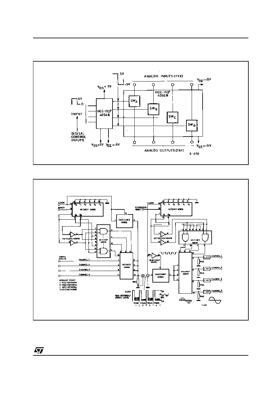
TYPICAL APPLICATIONS (BIDIRECTIONAL SIGNAL TRANSMISSION VIA DIGITAL CONTROL
LOGIC)
TYPICAL APPLICATIONS (4-CHANNEL PAM MULTIPLEXER SYSTEM DIAGRAM)