 | –≠–ª–µ–∫—Ç—Ä–æ–Ω–Ω—ã–π –∫–æ–º–ø–æ–Ω–µ–Ω—Ç: 420 | –°–∫–∞—á–∞—Ç—å:  PDF PDF  ZIP ZIP |

1/7
July, 3 2002
START420
NPN Silicon RF Transistor
SOT343 (SC70)
ORDER CODE
START420TR
BRANDING
420
APPLICATIONS
∑ LNA FOR GSM/DCS, DECT, PDC, PCS,
PCN
∑ PREDRIVER FOR DECT
∑ GENERAL PURPOSE 500MHz-5GHz
∑ LOW NOISE FIGURE: NFmin = 1.05dB
@ 1.8GHz, 5mA, 2V
∑ COMPRESSION P1dB = 12.5dBm
@ 1.8GHz, 20mA, 2V
∑ ULTRA MINIATURE SOT343 PACKAGE
DESCRIPTION
The START420 is a member of the START family
that provide market with the state of the art of RF
silicon process. Manufacturated in the third
generation of ST proprietary bipolar process, it
offers the best mix of gain and NF for given
breakdown voltage(BVceo).
It reaches performance level only achieved with
GaAs products before.
ABSOLUTE MAXIMUM RATINGS
Symbol
Parameter
Value
Unit
V
ceo
Collector emitter voltage
4.5
V
V
cbo
Collector base voltage
15
V
V
ebo
Emitter base voltage
1.5
V
I
c
Collector current
40
mA
I
b
Base current
4
mA
P
tot
Total dissipation, T
s
=
101
180
mW
T
stg
Storage temperature
-65 to 150
o
C
T
j
Max. operating junction temperature
150
o
C
R
thjs
Thermal Resistance Junction soldering point
270
o
C/W
ABSOLUTE MAXIMUM RATINGS
START420
2/7
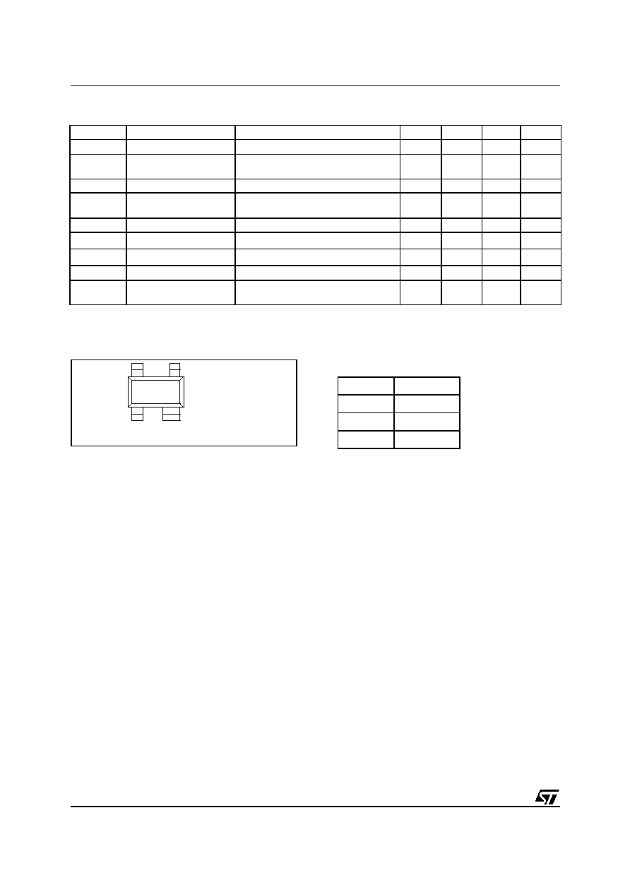
SOT343
4
1
2
3
Top view
Note(1): Gms = | S
21
/ S
12
|
Symbol
Parameter
Test Conditions
Min.
Typ.
Max.
Unit
I
cbo
Collector cutoff current
Vcb = 5V, Ie = 0A
150
nA
I
ebo
Emitter-base cutoff
current
Veb = 1.5V, Ic = 0A
15
µ
A
Hfe
DC current gain
Ic = 20mA, Vce = 3V
100
150
NFmin
Minimim noise figure
Ic = 5mA, Vce = 2V, f = 1.8GHz,
Z
s
= Z
s
opt
1.05
dB
Ga
NFmin associated gain
Ic = 5mA, Vce = 2V, f = 1.8GHz
16
dB
|S21|
2
Insertion power gain
Ic = 20mA, Vce = 2V, f = 1.8GHz
19.5
dB
Gms
(1)
Maximum stable gain
Ic = 20mA, Vce = 2V, f = 1.8GHz
22.6
dB
P
-1dB
1dB compression point
Ic = 20mA,Vce = 2V, f = 1.8GHz
12.5
dBm
OIP3
Ouput third order
intercept point
Ic = 20mA,Vce = 2V, f = 1.8GHz
23
dBm
ELECTRICAL CHARACTERISTICS (T
j
=25
o
C,unless otherwise specified)
PINOUT
PIN CONNECTION
Pin No.
Description
1
BASE
3
COLLECTOR
2,4
EMITTER
3/7
START420
Symbol
Value
Symbol
Value
Symbol
Value
TMEAS
27.0
FC
0.66
XJBC
0.53
IS
1.00E-16
EG
1.12
XTI
3.76
ISE
1.58E-11
NF
1
BF
280
NR
1
NE
3.1
VAF
70
ISC
1.55E-15
BR
9.52
VAR
2.3
IKF
{0.217*((T(
o
C)+273.15)/
300.15)^(-1.63)}
NC
1.495
TF
3.0E-12
TR
7E-10
PTF
32.0
VTF
27.9
XTF
9.84
ITF
0.498
MJE
0.497
RB
12.86
RBM
5
MJC
0.292
RC
3.7
RE
0.42
MJS
0.245
CJE
421E-15
VJE
1.03
IKR
8.32E-3
CJC
160E-15
VJC
0.6
XTB
-0.54
CJS
112E-15
VJS
0.4
SPICE PARAMETERS (Gummel-Poon Model, Berkley-SPICE 2G.6 Syntax)
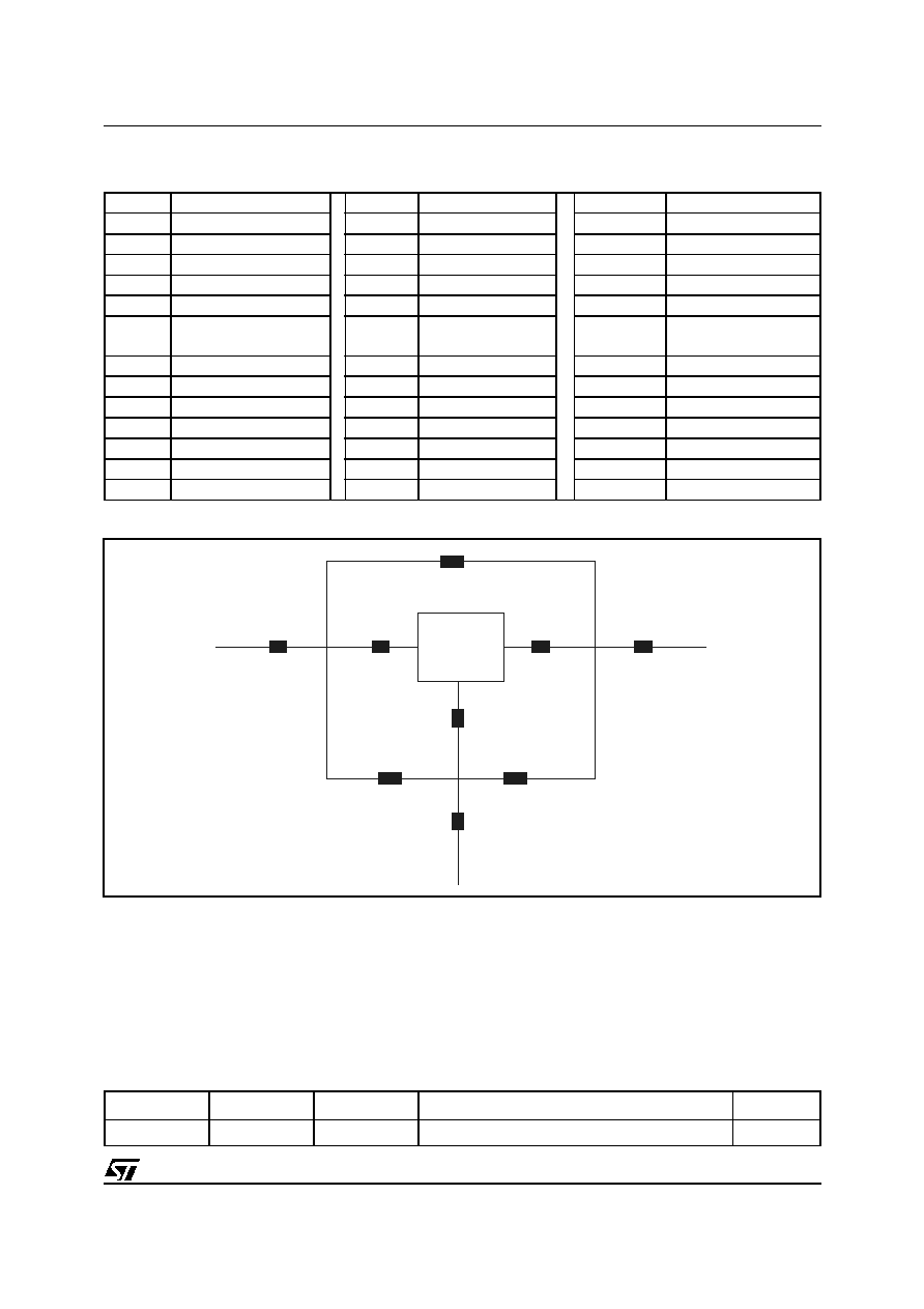
PACKAGE EQUIVALENT CIRCUIT
TRANSISTOR CHIP DATA
C
Transistor
Chip
B'
C'
E'
L=0.3 nH
L=0.6 nH
L3 L5
L6
C2
C=66 fF
. .
L=0.35 nH
L1
L=0.1 nH
L=0.05 nH
L2
C=334 fF
C=436 fF
C1
C3
E
.
.
L=0.6 nH
L4
B
.
.
FOR MORE ACCURACY SIMULATION IN SATURATION REGION :
Adding the 5 Spice parameters showed in Table A and using ST Spice Library (available on request) you
can achieve a more accuracy simulation in the saturation region. ST Spice library is compatible with
following simulators: ELDO MENTOR (any version), SPECTRE CADENCE (any version), ADS (version
2001 only).
Table A (Spice Parameters extracted in saturation region)
RW
Vjj
ENP
VRP
RP
1.173
0.8
2.085
{4.12*((TEMPER+273.15)/300.15)^(0.303)}
1.00E-6
In order to avoid high complexity of the package equivalent circuit, the two emitter leads of SOT-343
package are combined in one electrical connection.
START420
4/7
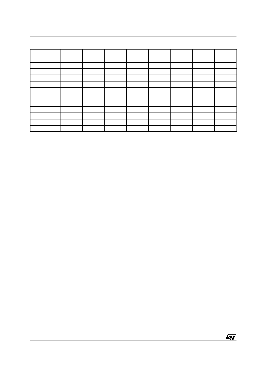
COMMON EMITTER S-PARAMETERS ( V
CE
= 2V, I
C
= 20mA )
FREQ
IS
11
I
IS
21
I
IS
12
I
S
12
IS
22
I
S
22
(MHz)
0.1
0.700
-22
42.223
164
0.010
89
0.932
-12
0.5
0.545
-90
27.116
120
0.027
58
0.632
-51
0.9
0.480
-130
18.322
98
0.036
48
0.421
-71
1
0.476
-137
16.756
94
0.038
47
0.387
-75
1.5
0.484
-167
11.532
77
0.048
42
0.263
-96
1.8
0.494
180
9.528
68
0.052
39
0.210
-111
2
0.503
172
8.390
63
0.055
37
0.183
-123
2.5
0.513
158
6.364
54
0.061
32
0.148
-154
3
0.533
148
4.936
46
0.069
27
0.143
-171
3.5
0.552
140
4.546
37
0.077
21
0.153
178
4
0.559
134
3.873
28
0.085
14
0.154
163
S
11
S
21

5/7
START420
TAPE & REEL DIMENSIONS
mm
MIN.
TYP.
MAX
A
178.5
179
179.5
C
12.8
13.0
13.5
D
20.2
N
54.5
55
55.5
T
14.4
Ao
2.25
Bo
2.7
Ko
1.2
Po
3.8 (cumulative 10 Po)
4.0
4.2 (cumulative 10 Po)
P
4.0
DEVICE ORIENTATION
TOP
VIEW END
VIEW
420
420
420
420