
October 1995
1/8
ST 486 DX ASIC CORE
Fully Static 3.3V 486 DX/DX2/DX4 ASIC CORE
PRELIMINARY DATA
s
Fully Static 486 compatible core able to
operate from D.C to 120MHz
s
Manufactured in a 0.35 micron five layer
metal HCMOS process
s
8K byte unified instruction and data cache
with write back capability
s
Parallel processing integral floating point unit,
with automatic power down mode
s
Low Power system management modes
s
Cell libraries for 2.2V and 3.3V supply with
5 V I/O interface capability
s
2 - input NAND delay of 0.160 ns (typ) with
fanout = 2.
s
Broad I/O functionality including LVCMOS,
LVTTL, GTL, PECL, and LVDS.
s
High drive I/O; capability of sinking up to 48
mA with slew rate control, current spike sup-
pression and impedance matching.
s
Generators to support SPRAM, DPRAM,
ROM and many other embedded functions.
s
Fully independent power and ground configu-
rations for inputs, core and outputs.
s
Programmable I/O ring capability up to 1000
pads.
s
Output buffers capable of driving ISA, EISA,
PCI, MCA, and SCSI interface levels.
s
Active pull up and pull down devices.
s
Buskeeper I/O functions.
s
Oscillators for wide frequency spectrum.
s
Broad range of 400 SSI cells.
s
Design For Test includes LSSD macro library
option and IEEE 1149.1 JTAG Boundary
Scan architecture built in.
s
Cadence based design system with inter-
faces from multiple workstations.
s
Broad ceramic and plastic package range.
s
Latchup trigger current > +/- 500 mA.
ESD protection > +/- 4000 volts.
AAAA
AAAA
AAAA
AAAA
AAAA
AAAA
AAAA
AAAA
AAAA
AAAA
AA
AA
AAAAAAAAAAAAAAAAAAAAAAA
AA
AA
AA
AAAA
AAAA
AAAA
AAAA
AAAA
AAAA
AAAA
AAAA
AAAA
AAAA
AA
AA
A
A
AAAA
AAAA
AAAA
AAAA
AAAA
AAAA
AAAA
AAAA
AAAA
AAAA
AAAA
AAAA
AAAA
AAAA
AAAA
AA
AA
AA
AAAA
AAAA
AAAA
AAAA
AAAA
AAAA
AAAA
AAAA
AAAA
AAAA
AAA
AAA
AA
AA
AA
AAAAAAAAAAAAAAAAAAAAAA
A
A
A
AAAA
AAAA
AAAA
AAAA
AAAA
AAAA
AAAA
AAAA
AAAA
AAAA
AAAA
AAAA
AAAA
AAAA
AAAA
AA
AA
AA
AAAA
AAAA
AAAA
AAAA
AAAA
AAAA
AAAA
AAAA
AAAA
AAAA
AAA
AAA
AA
AA
AA
AAAAAAAAAAAAAAAAAAAAAA
A
A
A
AAAA
AAAA
AAAA
AAA
AAA
AAA
AAA
AAAA
AAAA
AAAA
AAAA
AAAA
AAAA
AAAA
AAAA
AAA
AAA
AAA
AAA
AAA
AAA
AAA
AAA
AAA
AAA
AAA
AAAA
AAAA
AAAA
AAAA
AAA
AAA
AAA
AAAA
AAAA
AAAA
AAAA
AAA
AAA
AAA
AAA
AAA
AAA
AAA
AAA
AAAA
AAAA
AAAA
AAAA
AAAA
AAAA
AAAA
AAAA
AAAA
AAAA
AAAA
AAAA
AAA
AAA
AAA
AAA
AAA
AAA
AAA
AAAA
AAAA
AAAA
AAAA
AAA
AAA
AAA
AAA
AAA
AAA
AAA
AAA
AAAA
AAAA
AAAA
AAAA
AAAA
AAAA
AAAA
AAAA
AAAA
AAAA
AAAA
AAAA
AAA
AAA
AAA
AAA
AAAA
AAAA
AAAA
AAAA
AAAA
AAAA
AAAA
AAAA
AAAA
AAAA
AAAA
AAAA
AAAA
AAAA
AAAA
AAAA
AAAA
AAAA
AAAA
AAAA
AAAA
AAAA
AAAA
AAAA
AAAA
AAAA
AAAA
AAAA
AAAA
AAAA
AAAA
AAAA
AAAA
AAAA
AAAA
AAAA
AAAA
AAAA
AAAA
AAAA
AAAA
AAAA
AAAA
AAAA
AAAA
AAAA
AAAA
AAAA
AAAA
AAAA
AAAA
AAAA
AAAA
AAAA
AAAA
AAAA
AAAA
AAAA
AAAA
AAAA
AAAA
AAAA
AAAA
AAAA
AAAA
AAAA
AAAA
AAAA
AAAA
AAAA
AAAA
AAAA
AAAA
AAAA
AAAA
AAAA
AAAA
AAAA
AAAA
AAAA
AAAA
AAAA
AAAA
AAAA
AAAA
AAAA
AAAA
AAAA
AAAA
AAAA
AAAA
AAAA
AAAA
AAAA
AAAA
AAAA
AAAA
AAAA
AAAA
AAAA
AAAA
AAAA
AAAA
AAAA
AAAA
AAAA
AAAA
AAAA
AAAA
AAAA
AAAA
AAAA
AAAA
AAAA
AAAA
AAAA
AAAA
AAAA
AAAA
AAAA
AAAA
AAAA
AAAA
AAAA
AAAA
AAAA
AAAA
AAAA
AAAA
AAAA
AAAA
AAAA
AAAA
AAAA
AAAA
AAAA
AAAA
AAAA
AAAA
AAAA
AAAA
AAAA
AAAA
AAAA
AAAA
AAAA
AAAA
AAAA
AAAA
AAAA
AAAA
AAAA
AAAA
AAAA
AAAA
AAAA
AAAA
AAAA
AAAA
AAAA
AAAA
AAAA
AAAA
AAAA
AAAA
AAAA
AAAA
AAAA
AAAA
AAAA
AAAA
AAAA
AAAA
AAAA
AAAA
AAAA
AAAA
AAAA
AAAA
AAAA
AAAA
AAAA
AAAA
AAAA
AAAA
AAAA
AAAA
AAAA
AAAA
AAAA
AAAA
AAAA
AAAA
AAAA
AAAA
AAAA
AAAA
AAAA
AAAA
AAAA
AAAA
AAAA
AAAA
AAAA
AAAA
AAAA
AAAA
AAAA
AAAA
AAAA
AAAA
AAAA
AAAA
AAAA
AAAA
AAAA
AAAA
AAAA
AAAA
AAAA
AAAA
A
A
A
AAAA
AAAA
AAAA
AA
AA
AA
AAAA
AAAA
AAAA
AAAA
AAAA
AAAA
AAAA
AAAA
AAAA
AA
AA
AA
AAAA
AAAA
AAAA
AAAA
AAAA
AAAA
AAAA
AAAA
AAAA
AAAA
AAAA
AAAA
A
A
A
AAAA
AAAA
AAAA
AA
AA
AA
AAA
AAA
AAA
AAAA
AAAA
AAAA
AAAA
AAAA
AAAA
AA
AA
AA
AAAA
AAAA
AAAA
AAAA
AAAA
AAAA
A
A
A
AAA
AAA
AAA
AAA
AAA
AAA
AAA
AAA
AAA
AAA
AAA
AAA
AAA
AAA
AAA
AAA
AAA
AAA
AAA
AAA
AAA
AAA
AAA
AAA
AAA
AAA
AAA
AAA
AAA
AAA
AAA
AAA
AAA
AAA
AAA
AAA
AAA
AAA
AAA
AAA
AAA
AAA
AAA
AAA
AAA
AAA
AAA
AAA
AAA
AAA
AAA
AAA
AAA
AAA
AAA
AAA
AAA
AAA
AAA
AAA
AAA
AAA
S e a o f G at e s
S t a n d ar d C e l ls
C u s t o m I/ O
P r o g ra m m a b le
I/O
e .g R A M D A C
S V G A
C H IP S E T / P C I
ID E / IS A
4 8 6 D X C O R E
R O M
R A M
D P R A M
Figure 1. Example 486 DX Core ASIC

ST 486 DX ASIC CORE
2/8
�
PRODUCT OVERVIEW
The ST 486 DX core is based on the design of the
SGS-THOMSON standard 486 DX4 product. The
core is capable of operating at the "external" bus
speed or at two or three times the bus speed up to
a maximum of 120MHz. Since the design is fully
static the core can operate at any frequency
between D.C and 120MHz. The core is
manufactured on a high performance, low voltage,
five level metal, HCMOS 0.35 micron process to
achieve sub-nanosecond internal speeds while
offering very low power dissipation and high noise
immunity. The potential total gate count for
application specific devices exceeds 2 million
equivalent usable gates. The core operates over a
Vdd voltage range of 2.2 to 3.6 volts.
The core comes available with a full range of SSI,
MSI libraries as well as generators for SPRAM,
DPRAM, ROM. Where process and design
philosophy permit it is possible to integrate
existing "standard DEVICES" within a 486 core
design. A full set of "chipset" function blocks are
available to build support subsystems on chip
blocks such as IDE controller, PCI bridge, DRAM
controller etc.
The I/O can be configured for circuits ranging from
low voltage CMOS and TTL to 200 MHz plus low
swing differential circuits.
CLOCK-TRIPLED CPU CORE
The ST486DX Core in DX4 mode provides up to
2.8 times the performance of a 486DX at the same
"external" clock frequency. This level of
performance is achieved by tripling the frequency
of the input clock and using the resulting signal to
drive the CPU core. To further enhance this
architecture, the ST486DX Core reduces the
performance penalty of slow external memory
accesses through use of an on-chip write-back
cache and eight write buffers.
The CPU core consists of a five-stage pipeline
optimized for minimal instruction cycle times and
includes all necessary hardware interlocks to
permit successive instruction execution overlap.
The execution stage of the pipeline executes
simple but frequently used instructions in a single
clock cycle and the hardware multiplier executes
16-bit integer multiplications in only three clocks.
ON-CHIP WRITE-BACK CACHE
The ST486DX Core on-chip cache can be
configured to run in traditional write-through mode
or in a higher performance write-back mode. The
write-back cache mode was specifically designed
to optimize performance of the CPU core by
eliminating bus bottlenecks caused by
unnecessary external write cycles. This write-
back architecture is especially effective in
improving performance of the clock-tripled
ST486DX4 Core.
Traditional write-through cache architecture
require that all writes to the cache also update
external memory simultaneously. These
unnecessary write cycles create bottlenecks which
result in CPU stalls and adversely impact
performance. In contrast, a write-back
architecture allows data to be written to the cache
without updating external memory. With a write-
back cache, external write cycles are only required
when a cache miss occurs, a modified line is
replaced in the cache, or when an external bus
master requires access to data.
The ST486DX Core cache is an 8-Kilobyte unified
instruction and data cache implemented using a
four-way set associative architecture and a least
recently used (LRU) replacement algorithm. The
cache is designed for optimum performance in
write-back mode, however, the cache can be
operated in write-through mode. The cache line
size is 16 bytes and new lines are only allocated
during memory read cycles. Valid status is
maintained on a 16-byte cache line basis, but
modified or "dirty" status for write-back mode is
maintained on a 4-byte (double-word) basis.
Therefore, only the double-words that have been
modified are written back to external memory
when a line is replaced in the cache. The CPU
core can access the cache in a single internal
clock cycle for both reads and writes.
FPU OPERATIONS
Since the FPU is resident within the CPU, the
overhead associated with external maths
capriciousness cycles is eliminated. If the FPU is
not in use, the FPU is automatically powered
down. This feature reduces overall power
consumption.

3/8
ST 486 DX ASIC CORE
�
SYSTEM MANAGEMENT MODE
System Management Mode (SMM) provides an
additional interrupt and a separate address space
that can be used for system power management
or software transparent emulation of I/O
peripherals. SMM is entered using the System
Management Interrupt (SMI#) or SMINT
instruction. While running in isolated SMM
address space, the SMI interrupt routine can
execute without interfering with the operating
system or application programs.
After entering SMM, portions of the CPU state are
automatically saved. Program execution begins at
the base of SMM address space. The location
and size of the SMM memory are programmable
within the ST486DX Core. Eight SMM instructions
have been added to the 486 instruction set that
permit software entry into SMM, as well as saving
and restoring the total CPU state when in SMM
mode.
POWER MANAGEMENT
The ST486DX Core power management features
allow for a dramatic improvement in battery life
over systems designed with non-static 486
processors. During suspend mode the typical
current consumption is less than 1 percent of the
full operation current.
Suspend mode is entered by either a hardware or
a software initiated action. Using the hardware
method to initiate suspend mode involves a two-
pin handshake between the SUSP# and SUSPA#
signals. The software can initiate suspend mode
through the execution of the HALT instruction.
Once in suspend mode, the ST486DX Core power
consumption is further reduced by stopping the
external clock input. The resulting current draw is
typically 450 �A. Since the ST486DX Core is
static, no internal data is lost when the clock is
stopped.
SIGNAL SUMMARY
The ST486DX Core signal set includes ten cache
interface signals, two capriciousness interface
signals, two power management signals, two
system management mode signals, one power
supply voltage control signal and one clock
multiplier control signal.
LIBRARY
The following section details the elements which
make up the ST486DX core HCMOS6 library. The
elements are organised into three categories:
- Macrocell & Macrofunctions
- Module generators
- Embedded Functions
MACROCELLS AND MACROFUNCTIONS
The HCMOS 6 library has internal macrocells that
are robust in variety and performance. The cell
selection has been driven by the need of synthesis
and HDL based design techniques. This offering is
rich in buffers, complex combinatorial cells and
multi power drive cells, which allow the synthesis
tool to create a netlist compatible with the
requirements of Place and Route tools.
Macrofunctions are implemented at layout by
utilizing macrocells and interconnecting to create
the logic function. The Macrofunctions include all
the blocks needed to build a full PC chipset sub-
system.
Examples include DRAM controller, UART, DMA
controller, Interrupt Controller, Interval Timer, IDE
Controller, RTC, PCI Controller, MIDI port, etc.
MODULE GENERATORS
A series of module generators are available to
support a range of megafunctions. These modules
enable the designer to choose individual
parameters in order to create a compiled cell,
which meets the specific application requirements.
Generators are available for megafunctions such
as single port RAM and dual port RAM and ROM.
The compiled cell generators construct custom
cells, which are implemented using a special leaf
cell technique, ensuring predictable layout and
accurate module characteristics.
In choosing megafunctions the designer can
consider the trade-offs between speed and area to
generate a fully customized cell which meets their
specific device requirements.
EMBEDDED FUNCTIONS
Embedded megacells allow access to
technologies that have been hitherto the domain of
standard products.

ST 486 DX ASIC CORE
4/8
�
Examples include mixed mode cells for graphics,
DAC/ADC's (4-9 bit), PLL applications, and Digital
Signal Processor functions for cellular comms, fax
and high-speed modem. 100 Mbps serial
transputer links coupled with large and fast
memory can be used for pipelining, caching and
synchro circuits in modern CISC computing
architecture.
Viterbi and Reed Solomon cores aim at the HDTV
and satellite transmission markets. To support
telecom needs for CCITT standard applications,
ADPCM cells supporting CT2 protocol have been
developed. MPEG2 decoders interfacing directly
to the system memory are ideal for settop and
cable applications.
DESIGN FOR TESTABILITY
Using the internal test modes of the 486 core,
accessed through special test logic, the core
module can be thoroughly tested in `stand alone'
mode at both wafer sort and packaged die test.
The HCMOS 6 library supports the JTAG
boundary Scan and both edge and level sensitive
scan design techniques by providing the
necessary macrocells. Scan testing aids device
testability by permitting access to internal nodes
without requiring a separate external connection
for each node accessed. Testability is assured at
device level with the close coupling of LSSD latch
elements, Automatic Test Pattern Generation
(ATPG) and high pattern depth tester architecture.
At system level, SGS-THOMSON fully supports
IEEE 1149.1. Several types of core scan cells are
provided in the HCMOS 6 library.
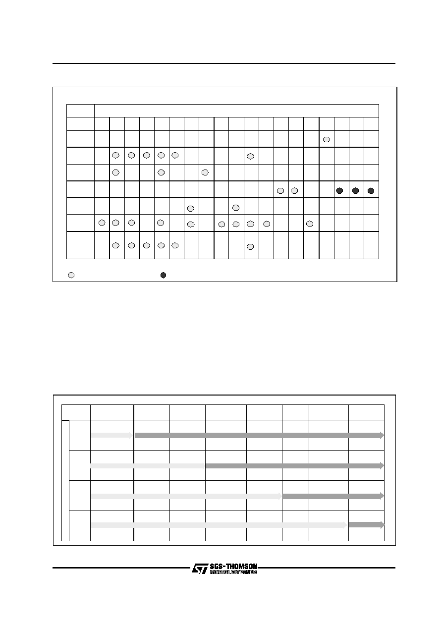
PACKAGE AVAILABILITY
The HCMOS 6 library is designed to be compatible
with QFP and BGA package types, in addition to
the more traditional types of package.
The options include Quad Flat Pack (xQFP)
offering ranges up to 304 pins. Both high
performance and high power variants are available
as well as the TQFP thin types.
Ball Grid Array (BGA) packages are available from
160 to 500 pins.
Pin counts for through board mounting range up to
299. For higher pin counts the range is compatible
with the industry standard JEDEC and EIA-J
Guardring Quad Flatpack (GQPF) with pin counts
from 186 to 304.
The diversity in pin count and package style gives
the designer the opportunity to find the best
compromise for system size, cost and
performance requirements.
DESIGN ENVIRONMENT
Several interface levels are possible between
SGS-THOMSON and the customer in the
undertaking of a 486 Core design. The four levels
of interface are shown in Figure 3. Level 1 is
characterized by SGS-THOMSON receiving the
system specification and taking the design through
to validation and fabrication. At level 2 interface
the designer supplies a simulated netlist at the
RTL HDL level. SGS-THOMSON then takes the
design through synthesis and gate level simulation
to layout, validation and fabrication.
Level 3 the designer completes the design to final
gate level simulation. The design is then taken
through layout, validation and fabrication by SGS-
THOMSON.
At level 4 the designer completes all of the design
and layout and supplies the design database to
SGS-THOMSON in GDS 2 format. SGS-
THOMSON will then complete LVS and DRC and
generate the PG tape for mask generation and
fabrication.
TECHNOLOGY
For this product, a high performance, low voltage,
five level metal, salicided poly and diffusion
HCMOS 0.35 micron process has been used to
achieve sub-nanosecond internal speeds while
offering very low power dissipation and high noise
immunity.
Its fabrication involve more than 140 elementary
operations, including selective tungsten vias,
plasma interment dielectric deposition and CMP
(Chemical-Mechanical Planarization) for the
incrementally oxides.
METHODOLOGY
The design environment for x86 embedded
products has been designed for maximum
flexibility and reliability, and has been based on
typical ASIC like design flows using HDL and
Synthesis methodologies.
5/8
ST 486 DX ASIC CORE
�
SIMULATION ENVIRONMENT
The key area of the design flow is the simulation
environment that allows for multiple levels of
design abstraction to be simulated concurrently.
The Cadence Leapfrog/Verilog-XL simulation
engine has been chosen for this "mix and match"
approach, allowing for gate level functional and
timing verification for individual modules to be
performed within a high level description of the
entire device.
CORE MODELS
The ST486DX core can be represented in the
simulation environment through different model
types such as a VHDL bus functional model or a
Model Source hardware model. The Model Source
option utilises ST486DX silicon interfaced to the
VHDL/Verilog software co-simulation environment
through a software shell.
SY ST EM
SY ST EM
SP E C IFIC A TION
BE H A VIO R AL
H D L
R TL H D L
SY N TH E SIS
PRE-L AYO UT
G ATE L EVEL
SIM U LATION
LA Y OU T
PO ST-LAYO U T
G ATE L EVEL
SIM U LATION
M AN U FA C T.
AN D TES T
L EV EL
1
C U ST O M E R
L EV EL
2
L EV EL
3
L EV EL
4
I
N
T
E
R
F
A
C
E
L
EVEL
S
SG S-TH O M SO N
SG S-T H O M SO N
SG S-TH O M SO N
SG S-T H O M SO N
C U STO M ER
C U STO M E R
C U STO M ER
Figure 3. Customer Interfaces
PACKAGE
NAME
84
100
120
128
144
160
168
176
180
196
208
224
225
256
257
304
313
400
480
GQ FP
PQFP
TQFP
BGA
Plastic
PGA
CP GA
POW
PQFP
with Slug
or
Spreader
: Packages in production : Packages in development
NUMBER OF LEADS (Pins)
PACKAGE OPTIONS
Figure 2. Standard Package Options