 | –≠–ª–µ–∫—Ç—Ä–æ–Ω–Ω—ã–π –∫–æ–º–ø–æ–Ω–µ–Ω—Ç: 57C51C-70 | –°–∫–∞—á–∞—Ç—å:  PDF PDF  ZIP ZIP |
PRODUCT SELECTION GUIDE
PARAMETER
57C51C-35
57C51C-45
57C51C-55
57C51C-70
Address Access Time (Max)
35 ns
45 ns
55 ns
70 ns
CS to Output Valid Time (Max)
20 ns
20 ns
25 ns
30 ns
WS57C51C
2-47
HIGH SPEED 16K x 8 CMOS PROM/RPROM
KEY FEATURES
∑
Very Fast Access Time
∑
Pin Compatible with Am27S51
--
35 ns
and N82HS1281
∑
Low Power Consumption
∑
Immune to Latch-Up
∑
Fast Programming
--
Up to 200 mA
∑
ESD Protection Exceeds 2000 V
GENERAL DESCRIPTION
The WS57C51C is a High Performance 128K UV Erasable Electrically Re-Programmable Read Only Memory
(RPROM). It is manufactured in an advanced CMOS technology which enables it to operate at Bipolar PROM
speeds while consuming only 25% of the power required by its Bipolar counterparts.
A further advantage of the WS57C51C over Bipolar PROM devices is the fact that it utilizes a proven EPROM
technology. This enables the entire memory array to be tested for switching characteristics and functionality after
assembly. Unlike devices which cannot be erased, every WS5751C in a windowed package is 100% tested with
worst case test patterns both before and after assembly.
The WS57C51C provides a low power alternative to those designs which are committed to a Bipolar PROM
footprint. It is a direct drop-in replacement for a Bipolar PROM of the same architecture (16K x 8). No software,
hardware or layout changes need be performed.
V
CC
A10
A11
A12
A13
CS1/VPP
CS2
CS3
CS4
O
7
O
6
O
5
O
4
O
3
A
9
A
8
A
7
A
6
A
5
A
4
A
3
A
2
A
1
A
0
O
0
O
1
O
2
GND
1
2
3
4
5
6
7
8
9
10
11
12
13
14
28
27
26
25
24
23
22
21
20
19
18
17
16
15
A
12
A
13
CS1/V
PP
CS2
CS3
CS4
NC
O
7
O
6
A
5
A
4
A
3
A
2
A
1
A
0
NC
O
0
O
1
A
6
A
7
A
8
A
9
V
CC
A
10
A
11
O
2
NC
O
3
NC
O
4
O
5
1
4 3
2
32 31 30
29
28
27
26
25
24
23
22
21
5
6
7
8
9
10
11
12
13
14 15 16 17 18 19 20
GND
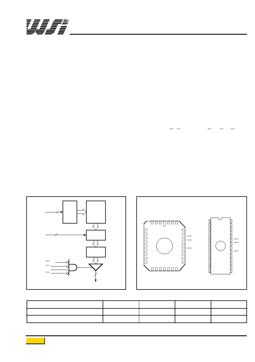
TOP VIEW
Chip Carrier
CERDIP
PIN CONFIGURATION
ROW
DECODER
EPROM ARRAY
131,072 BITS
COLUMN
DECODER
SENSE
AMPLIFIERS
8
CS3
CS4
OUTPUTS
CS1/ V
PP
A0 - A5
COLUMN
ADDRESSES
A6 - A13
ROW
ADDRESSES
8
6
CS2
BLOCK DIAGRAM
Return to Main Menu
WS57C51C
2-48
OPERATING RANGE
RANGE
TEMPERATURE
V
CC
Commercial
0∞C to +70∞C
+5V ± 10%
Industrial
≠40∞C to +85∞C
+5V ± 10%
Military
≠55∞C to +125∞C
+5V ± 10%
ABSOLUTE MAXIMUM RATINGS*
Storage Temperature............................≠65∞ to + 150∞C
Voltage on any Pin with
Respect to Ground ....................................≠0.6V to +7V
V
PP
with Respect to Ground...................≠0.6V to + 14V
ESD Protection ..................................................
>
2000V
NOTES:
1. CMOS inputs: GND ± 0.3V or V
CC
± 0.3V.
2. TTL inputs: V
IL
0.8V, V
IH
2.0V.
3. These are absolute voltages with respect to device ground pin and include all overshoots due to system and/or tester noise.
Do not attempt to test these values without suitable equipment.
*
NOTICE:
Stresses above those listed under "Absolute Maximum
Ratings" may cause permanent damage to the device.
This is a stress rating only and functional operation of
the device at these or any other conditions above
those indicated in the operational sections of this
specification is not implied. Exposure to absolute
maximum rating conditions for extended periods of
time may affect device reliability.
PINS
CS1/
MODE
VPP
CS2 CS3 CS4 V
CC
OUTPUTS
Read
V
IL
V
IL
V
IH
V
IL
V
CC
D
OUT
Output
Disable
V
IH
X
X
X
V
CC
High Z
Output
X
V
IH
X
X
V
CC
High Z
Disable
Output
X
X
V
IL
X
V
CC
High Z
Disable
Output
X
X
X
V
IH
V
CC
High Z
Disable
Program
V
PP
V
IH
X
X
V
CC
D
IN
Program
Verify
V
IL
V
IL
V
IH
V
IL
V
CC
D
OUT
MODE SELECTION
DC READ CHARACTERISTICS
Over Operating Range. (See Above)
SYMBOL
PARAMETER
TEST CONDITIONS
MIN
MAX
UNITS
V
IL
Input Low Voltage
(Note 3)
≠0.1
0.8
V
V
IH
Input High Voltage
(Note 3)
2.0
V
CC
+ 0.3
V
V
OL
Output Low Voltage
I
OL
= 16 mA
0.4
V
V
OH
Output High Voltage
I
OH
= ≠4 mA
2.4
V
V
CC
= 5.5 V, f = 0 MHz (Note 1),
Comm'l
30
mA
I
CC1
V
CC
Active Current
Output Not Loaded
Industrial
35
mA
(CMOS)
Add 4 mA/MHz for AC Operation
Military
35
mA
V
CC
= 5.5 V, f = 0 MHz (Note 2),
Comm'l
50
mA
I
CC2
V
CC
Active Current
Output Not Loaded
Industrial
60
mA
(TTL)
Add 4 mA/MHz for AC Operation
Military
60
mA
I
LI
Input Leakage
Current
V
IN
= 5.5V or Gnd
≠10
10
µA
I
LO
Output Leakage
Current
V
OUT
= 5.5 V or Gnd
≠10
10
µA
AC READ CHARACTERISTICS
Over Operating Range. (See Above)
PARAMETER
SYMBOL
57C51C-35
57C51C-45
57C51C-55
57C51C-70
UNITS
MIN
MAX
MIN
MAX
MIN
MAX
MIN
MAX
Address to Output Delay
t
ACC
35
45
55
70
CS to Output Delay
t
CS
20
20
25
30
ns
Output Disable to
Output Float
*
t
DF
20
20
25
25
Address to Output Hold
t
OH
0
0
0
0
*
Sampled, Not 100% Tested.
WS57C51C
2-49
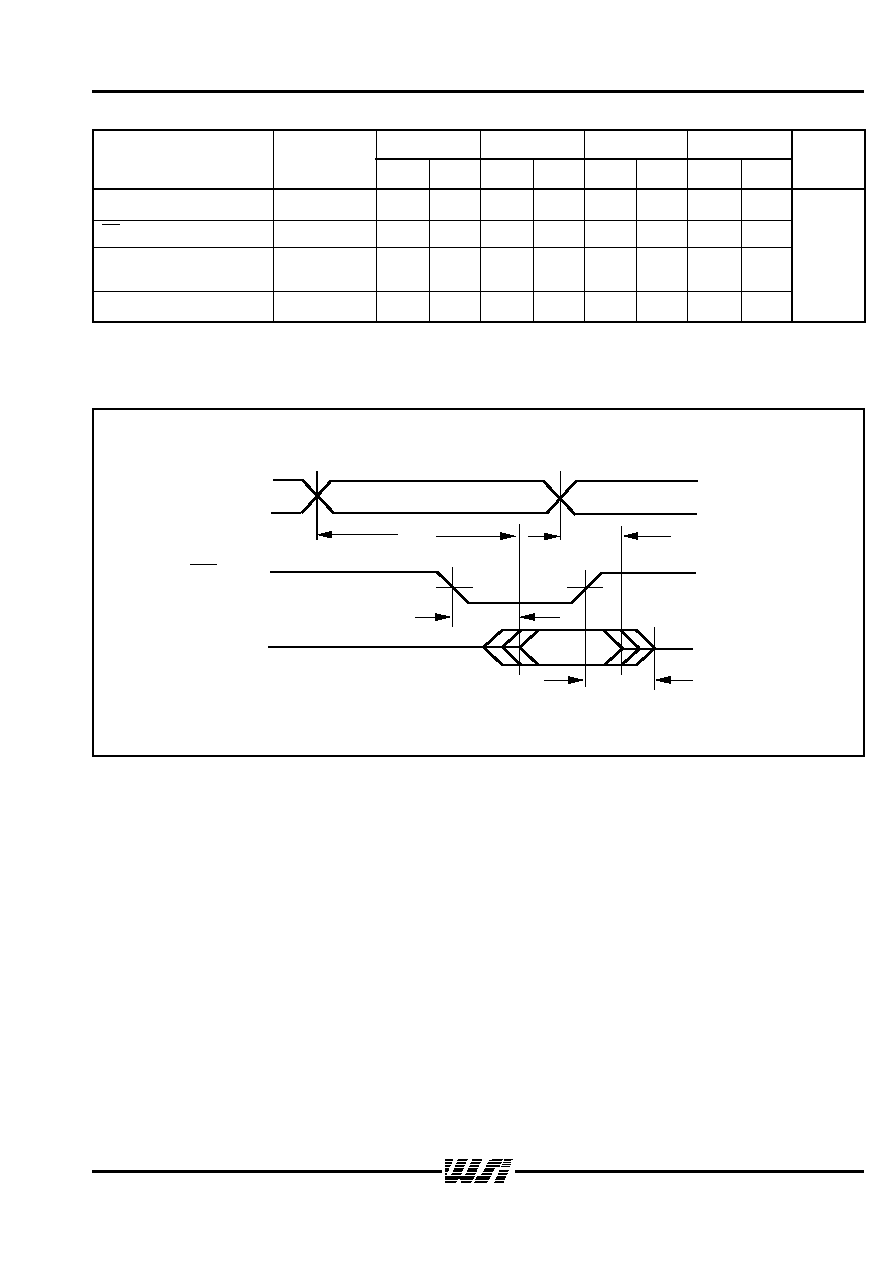
AC READ TIMING DIAGRAM
VALID
ADDRESSES
OUTPUTS
t
ACC
t
OH
t
CS
t
DF
VALID
CSX, CS3
WS57C51C
2-50
SYMBOL
PARAMETER
CONDITIONS
TYP
(5)
MAX
UNITS
C
IN
Input Capacitance
V
IN
= 0V
4
6
pF
C
OUT
Output Capacitance
V
OUT
= 0V
8
12
pF
C
VPP
V
PP
Capacitance
V
PP
= 0 V
18
25
pF
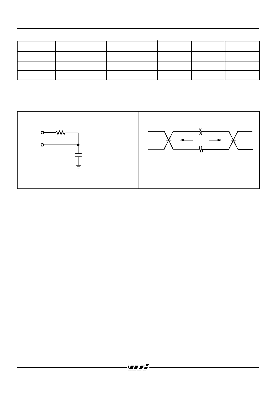
CAPACITANCE
(4)
T
A
= 25∞C, f = 1 MHz
30 pF
(INCLUDING SCOPE
AND JIG
CAPACITANCE)
98
2.01 V
D.U.T.
A.C. TESTING INPUT/OUTPUT WAVEFORM
TEST LOAD
(High Impedance Test Systems)
3.0
0.0
1.5
1.5
TEST
POINTS
NOTE: 6. Provide adequate decoupling capacitance as close as possible to this device to achieve the published A.C. and D.C. parameters.
A 0.1 microfarad capacitor in parallel with a 0.01 microfarad capacitor connected between V
CC
and ground is recommended.
Inadequate decoupling may result in access time degradation or other transient performance failures.
NOTES: 4. This parameter is only sampled and is not 100% tested.
5.Typical values are for T
A
= 25∞C and nominal supply voltages.
A.C. testing inputs are driven at 3.0 V for a logic "1" and 0.0 V
for a logic "0." Timing measurements are made at 1.5 V for
input and output transitions in both directions.
2-51
WS57C51C
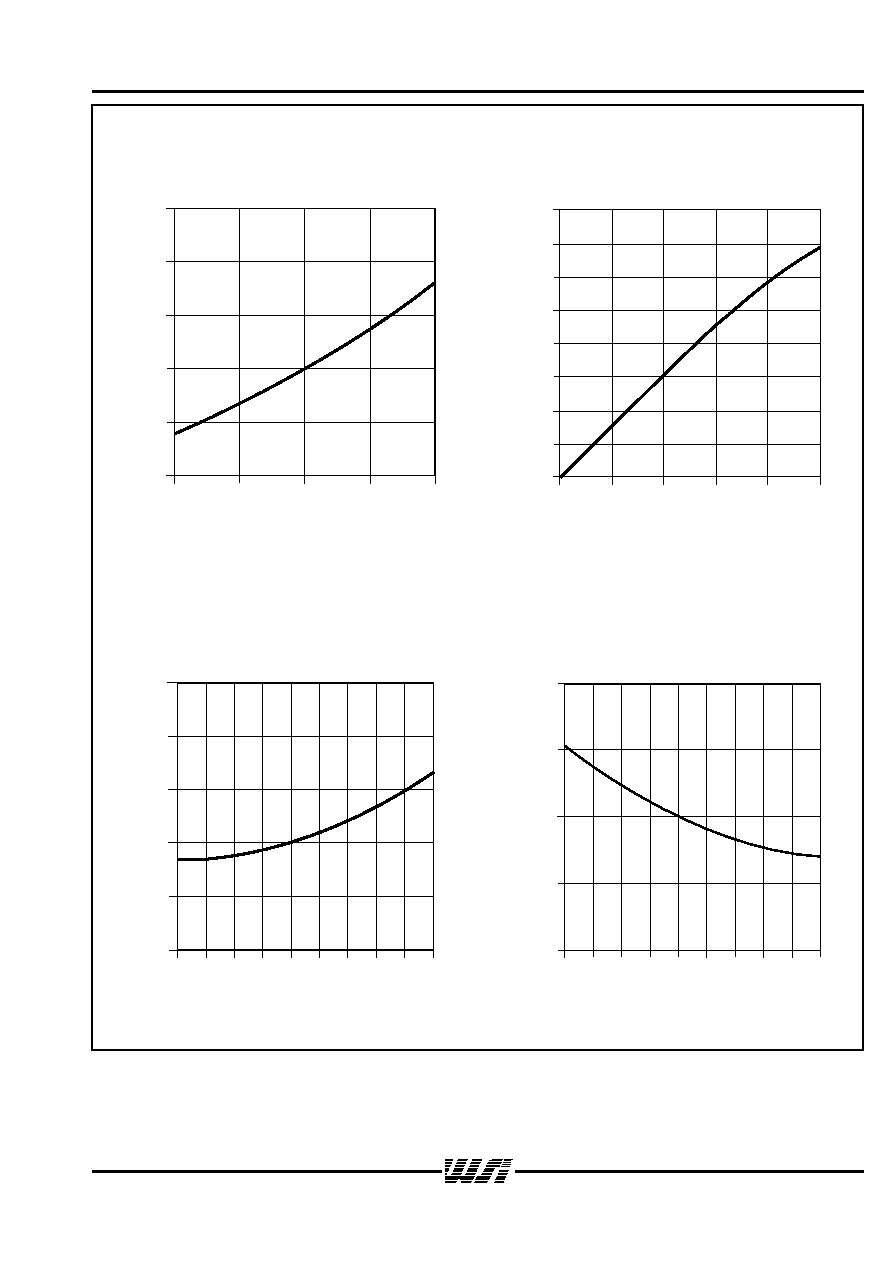
1.2
1.1
1.0
0.9
0.8
-55 -35 -15
5
25
45
65
85
105 125
AMBIENT TEMPERATURE (∞C)
NORMALIZED I
CC
1.60
1.40
1.20
1.00
0.80
0.60
4.0
4.5
5.0
5.5
6.0
SUPPLY VOLTAGE ( V )
NORMALIZED I
CC
1.6
1.4
1.2
1.0
0.8
0.6
-55 -35
-15
5
25
45
65
85
105 125
AMBIENT TEMPERATURE (∞C)
NORMALIZED T
aa
40.0
35.0
30.0
25.0
20.0
15.0
10.0
5.0
0.0
0.0
200
400
600
800
1000
CAPACITANCE ( pF)
DELTA T
aa
(
ns
)
NORMALIZED SUPPLY CURRENT
vs.
SUPPLY VOLTAGE
TYPICAL ACCESS TIME CHANGE
vs.
OUTPUT LOADING
NORMALIZED Taa
vs.
AMBIENT TEMPERATURE
NORMALIZED SUPPLY CURRENT
vs.
AMBIENT TEMPERATURE