 | –≠–ª–µ–∫—Ç—Ä–æ–Ω–Ω—ã–π –∫–æ–º–ø–æ–Ω–µ–Ω—Ç: 7003 | –°–∫–∞—á–∞—Ç—å:  PDF PDF  ZIP ZIP |
1/9
January, 22 2002
STB7003
TRI-BAND GSM/DCS/PCS LNA
MSOP10-EP
(exposed pad)
ORDER CODE
STB7003
BRANDING
7003
∑ SUPPLY VOLTAGE 2.8V
∑ LOW CURRENT CONSUMPTION
∑ VERY LOW NOISE FIGURE:
NF=1.5dB @ 950MHz
NF=1.9dB @ 1850MHz
NF=2dB @ 1950MHz
∑ DIGITAL GAIN CONTROL
APPLICATIONS
TRI-BAND GSM/DCS/PCS FRONT-ENDS
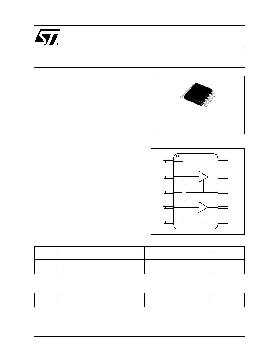
DESCRIPTION
The STB7003 is a tri-band LNA designed for GSM/DCS/
PCS applications. The GC pin sets the LNA gain levels.
The innovative architecture implemented allows to
reach very low current consumption. LNA1 works at
0.9-1.0 GHz and LNA2 over the 1.8-2GHz frequency
range.
FUNCTIONAL BLOCK DIAGRAM
GC
LNA2
BI
A
S
LNA1
AO2
Vcc
GSM
AO1
Vcc
DCS
PD
AI2
GND
AI1
BSW
ABSOLUTE MAXIMUM RATING
Symbol
Parameter
Value
Unit
Vcc
Supply voltage
4.5
V
Tj
Junction temperature
150
o
C
T
stg
Storage temperature
-40 to +85
∞C
THERMAL DATA
Symbol
Parameter
Value
Unit
R
th(j-a)
Thermal resistance junction-ambient
TBD
o
C/W

STB7003
2/9
ELECTRICAL CHARACTERISTICS (Vcc = 2.8V, Tamb= 25
o
C)
Symbol
Parameter
Test conditions
Min.
Typ.
Max.
Unit
Vcc
Supply voltage
2.7
3.3
V
I
PD
Sleep supply current
5
uA
LNA1 @ 950MHz
Icc
Supply current
4.5
mA
G
Power gain
G
p1
(1)
G
p2
(1)
-1
16
dB
NF
Noise figure
G
p1
G
p2
5.5
1.5
dB
P1dB
Input 1 dB compr.
power
G
p1
G
p2
-19
-21
dBm
IIP3
Input third order
intercept
G
p1
(2)
G
p2
(2)
-10.8
-12.6
dBm
VSWRi
Input VSWR
2:1
VSWRo
Output VSWR
2:1
LNA2 @ 1850MHz
Icc
Supply current
7.3
mA
G
Power gain
G
p1
(1)
G
p2
(1)
-4
14.7
dB
NF
Noise figure
G
p1
G
p2
9.6
1.9
dB
P1dB
Input 1 dB compr.
power
G
p1
G
p2
-11.5
-13.1
dBm
IIP3
Input third order
intercept
G
p1
(3)
G
p2
(3)
-1.4
-3.5
dBm
VSWRi
Input VSWR
2:1
VSWRo
Output VSWR
2:1
LNA2 @ 1950MHz
Note(1) : Gp1 min gain, Gp2 max gain.
Note(2) : Measured data with two tones f
IN1
= 945 MHz, f
IN2
= 945.8 MHz, P
IN
= - 33 dBm for each tone
Note(3) : Measured data with two tones f
IN1
= 1850 MHz, f
IN2
= 1850.8 MHz, P
IN
= - 33 dBm for each tone
Note(4) : Measured data with two tones f
IN1
= 1960 MHz, f
IN2
= 1960.8 MHz, P
IN
= - 33 dBm for each tone
Icc
Supply current
7.3
mA
G
Power gain
G
p1
(1)
G
p2
(1)
-4.5
14.7
dB
NF
Noise figure
G
p1
G
p2
9.8
2
dB
P1dB
Input 1 dB compr.
power
G
p1
G
p2
-10.8
-12.6
dBm
IIP3
Input third order
intercept
G
p1
(4)
G
p2
(4)
-1.5
-3.7
dBm
VSWRi
Input VSWR
2:1
VSWRo
Output VSWR
2:1

3/9
STB7003
GAIN SELECTION
PINOUT
BSW
GC
GSM
LNA1
DCS/PCS
LNA2
0
0
High gain
Off
0
1
Low gain
Off
1
0
Off
High gain
1
1
Off
Low gain
Pin Number
Symbol
Description
1
PD
Power down
2
AI1
GSM LNA1 input
3
GND
Ground
4
AI2
DCS/PCSl LNA2 input
5
BSW
Band switch between GSM and DCS/PCS RF output
6
Vcc
DCS
DCS Supply voltage
7
AO2
DCS/PCS LNA2 output
8
Vcc
GSM
GSM/BiAS Supply voltage
9
AO1
GSM LNA1 output
10
GC
LNA1/2 gain control
STB7003
4/9
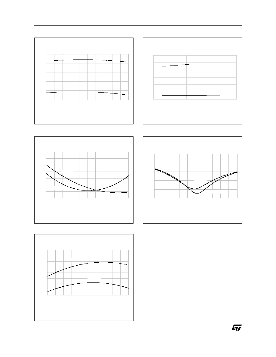
TYPICAL PERFORMANCE (GSM BAND)
Power Gain
vs. Frequency
Noise Figure vs. Frequency
920
930
940
950
960
970
Frequency (MHz)
1
2
3
4
5
6
7
NF (d
B
)
Low Gain
High Gain
Power Gain
vs. Frequency
-5
0
5
10
15
20
800
820
840
860
880
900
920
940
960
980 1000
High Gain
Low Gain
FREQUENCY (MHz)
S21(
Log M
ag)
(
d
B
)
Output Return Loss vs. Frequency
-25
-20
-15
-10
-5
0
800
820
840
860
880
900
920
940
960
980 1000
FREQUENCY (MHz)
RE
TURN L
O
S
S
High Gain
Low Gain
Input Return Loss vs. Frequency
-14
-12
-10
-8
-6
-4
-2
0
800
820
840
860
880
900
920
940
960
980
1000
RE
TURN L
O
S
S
(
d
B
)
FREQUENCY (MHz)
0
Low Gain
HIgh Gain
Reverse Isolation vs. Frequency
-48
-47
-46
-45
-44
-43
-42
-41
-40
800
820
840
860
880
900
920
940
960
980 1000
FREQUENCY (MHz)
S21(
Log M
ag)
(
d
B
)
HIgh Gain
Low Gain

5/9
STB7003
TYPICAL PERFORMANCE (DCS / PCS BAND)
Power Gain
vs. Frequency
-10
-5
0
5
10
15
20
1800 1820 1840 1860 1880 1900 1920 1940 1960 1980 2000
S21(
Log M
ag)
(
d
B
)
FREQUENCY (MHz)
Low Gain
High Gain
Noise Figure vs. Frequency
1800
1850
1900
1950
2000
FREQUENCY (MHz)
1
2
3
4
5
6
7
8
9
10
11
NF (d
B
)
Low Gain
High Gain
Input Return Loss vs. Frequency
-20
-18
-16
-14
-12
-10
-8
-6
-4
-2
0
1800 1820 1840 1860 1880 1900 1920 1940 1960 1980 2000
RE
TURN L
O
S
S
High Gain
Low Gain
FREQUENCY (MHz)
Reverse Isolation
vs. Frequency
-44
-43
-42
-41
-40
-39
-38
-37
-36
-35
1800 1820 1840 1860 1880 1900 1920 1940 1960 1980 2000
FREQUENCY (MHz)
S12 (
Log M
ag)
(
d
B
)
High Gain
Low Gain
Output Return Loss vs. Frequency
-12
-10
-8
-6
-4
-2
0
1800 1820 1840 1860 1880 1900 1920 1940 1960 1980 2000
FREQUENCY (MHz)
RE
TURN L
O
S
S
(
d
B
)
Low Gain
High Gain