 | –≠–ª–µ–∫—Ç—Ä–æ–Ω–Ω—ã–π –∫–æ–º–ø–æ–Ω–µ–Ω—Ç: 7404 | –°–∫–∞—á–∞—Ç—å:  PDF PDF  ZIP ZIP |
1/11
November 2000
s
ONLY TWO CELL NEED AS INPUT
s
THREE REGULATED OUTPUT
1) HIGH EFFICENCY PFM DC/DC
CONVERTER 3.3V AT 200mA (87%
EFFICENCY)
2) VERY LOW NOISE AND VERY LOW
DROP V
REG
(3V AT 20mA)
3) VERY LOW NOISE AAND VERY LOW
DROP V
REG
(1.9V AT 20mA)
s
LOGIC CONTROLLED ELECTRONIC
SHUTDOWN
s
LOW BATTERY DETECTOR
s
VIRTUAL GND PIN
s
TEMPERATURA RANGE: -40 TO 85∞C
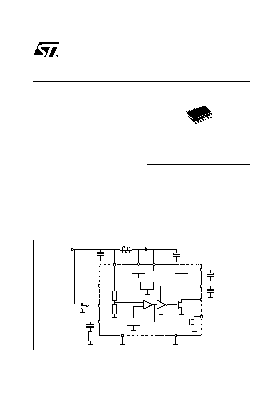
ST3M01
TRIPLE VOLTAGE REGULATOR
SHDN
DC/DC
Linear A
Linear B
IN_Linear
OUT DC/DC
OUT LA
OUT LB
150 µF
1 µF
15 µH
DC/DC
Ref
Ref
Vref
Lx
Virtual GND
100 nF
GND_SW
-
+
GND_Signal
IN_SW
Vin
150 µF
1 µF
1 K
LBO
On-Mode
Off-Mode
SCHEMATIC DIAGRAM
SO-14
ST3M01
2/11
ABSOLUTE MAXIMUM RATINGS
THERMAL DATA
ORDER CODES
Symbol
Parameter
Value
Unit
V
IN
DC Input Voltage (Both IN_Linear and IN_SW)
-0.3 to 7
V
V
SHDN
Shutdown Input Voltage
-0.3 to V
IN
+0.3
V
V
LX
Switch Voltage
-0.3 to 7
V
V
LBO
Low Battery Output Voltage
-0.3 to 7
V
V
virtual_GND
Virtual GND Output Voltage
-0.3 to 7
V
I
LBO
Low Battery Output Maximum Current
30
mA
I
virtual_GND
Virtual GND Output Maximum Current
30
mA
T
stg
Storage Temperature Range
-65 to +150
∞C
T
op
Operating Junction Temperature Range
-40 to +85
∞C
Symbol
Parameter
Value
Unit
R
thj-amb
Thermal Resistance Junction-ambient (*)
160
∞C/W
Type
Package
Comment
ST3M01D
SO-14
50 parts per tube / 20 tube per box
ST3M01DTR
SO-14 (Tape & Reel)
2500 parts per reel

ST3M01
3/11
CONNECTION DIAGRAM (top view)
PIN DESCRIPTION
Pin N∞
Symbol
Name and Function
1
GND SW
Switching Ground. Must be low impedance; solder directly to GND plane
2
GND SW
Switching Ground. Must be low impedance; solder directly to GND plane
3
Virtual GND
Virtual GND. Open Drain N-Cnannel MOSFET: must be high impedance when the
Low Battery condition is detected.
4
LBO
Low Battery Output. Open Drain N-Cnannel MOSFET: sinks current when the
input voltage drops below 2V typically.
5
V
REF
Reference Voltage Output. Bypass with 0.1
µ
F to improve the linears V
REF
thermal noise performance
.
6
IN Linear
Linear Input. Must be connected togheter with IN SW to the input supply.
7
OUT L
B
Linear B Output port. 1.9V typically.
8
SHDN
Shutdown Input. Disables the SMPS and
L
A
output, but the
L
B
, the
referencevoltage and the low batery comparator remain active.
9
GND Signal
Signal GND. Must be connected togheter with the Switching Ground.
10
OUT L
A
Linear A Output port. 3V typically.
11
OUT DC/DC
DC/DC Output Port: 3.3V typically.
12
IN SW
SMPS Input. Must be connected togheter with IN_Linear to the input supply.
13
LX
1.5A N-Channel Power MOSFET Drain.
14
LX
1.5A N-Channel Power MOSFET Drain.

ST3M01
4/11
ELECTRICAL CHARACTERISTICS (Unless otherwise specified, please refer to the typical operating
circut of the pag 1 for the external components values and connections. Unless otherwise noted
V
SHDN
=HIGH)
Note 1: For V
IN
< 1.9V the V
O(LB)
is out of regulation because of under dropout condition
Note 2: V
O(DC/DC)
= 3.5V force for an external DC source to avoid switching noise
Symbol
Parameter
Test Conditions
Min.
Typ.
Max.
Unit
V
I
Operating Input Voltage
1.9
3.3
V
V
O(DC/DC)
DC/DC Converter Output
Voltage (Test Circuit A)
2.24<V
IN
<3.3V; 0<I
O(DC/DC)
<200mA;
0<I
O(LA)
<20mA; 0<I
O(LB)
<20mA;
-40 < T
J
< 85 ∞C
3.2
3.3
3.415
V
DC/DC Converter Efficency V
IN
=2.4V; I
O(DC/DC)
=100mA;
I
O(LA)
=0mA; I
O(LB)
=0mA; T
J
= 25∞C
87
%
V
O(LA)
Linear A Output Voltage
(Test Circuit A)
2.24<V
IN
<3.3V; 0<I
O(DC/DC)
<200mA;
0<I
O(LA)
<20mA; 0<I
O(LB)
<20mA;
-40 < T
J
< 85∞C
2.93
3
3.09
V
V
O(LB)
Linear B Output Voltage
(Test Circuit A)
2.24<V
IN
<3.3V; 0<I
O(DC/DC)
<200mA;
0<I
O(LA)
<20mA; 0<I
O(LB)
<20mA;
-40 < T
J
< 85∞C
1.86
1.9
1.955
V
e
N(LA)
Linear A Thermal Output
Noise Voltage (Note 2)
V
IN
=2.4V; V
O(DC/DC)
=3.5V;
I
O(LA)
=20mA;
10 < f < 80KHz;
C
O(LA)
=1
µ
F; C
REF
=0.1
µ
F; T
J
= 25∞C
60
µ
V
rms
e
N(LB)
Linear B Thermal Output
Noise Voltage (Note 2)
V
IN
=2.4V; V
O(DC/DC)
=3.5V;
I
O(LB)
=20mA;
10 < f < 80KHz;
C
O(LB)
=1
µ
F; C
REF
=0.1
µ
F; T
J
= 25∞C
35
µ
V
rms
I
q(OFF)
Quiescent Current OFF
Mode DC/DC & L
A
OFF L
B
ON) (Test Circuit E)
V
IN
=3.3V;
No Load;
V
SHDN
=LOW;
T
J
= 25∞C
75
µ
A
I
q(OFF)
Quiescent Current OFF
Mode (DC/DC & L
A
OFF L
B
ON) (Test Circuit F)
V
IN
=1.9V;
No Load;
V
SHDN
=HIGH;
T
J
= 25∞C
50
µ
A
I
S(DC/DC)
DC/DC Supply Current
(Test Circuit B)
V
IN
=2.24V; No
Load; T
J
= 25∞C
100
µ
A
I
q(LA)
Linear A Quiescent Current
(Test Circuit C)
V
IN
=2.24V; V
O(DC/DC)
=3.5V;
I
O(LA)
=10mA; T
J
= 25∞C
220
µ
A
I
q(LB)
Linear B Quiescent Current
(Test Circuit C)
V
IN
=2.24V; V
O(DC/DC)
=3.5V;
I
O(LB)
=10mA; T
J
= 25∞C
75
µ
A
V
BATT
Low Battery Detection
Range
V
SHDN
=HIGH with falling edge
1.96
2
2.04
V
V
BATT(HYS)
Low Battery Detection
Hysteresys
150
200
mV
R
ON(LBO)
LBO R
DSON
V
IN
=1.9V; I
D
=5mA; T
J
= 25∞C
10
V
ih
Control Input Logic Low
V
IN
>2.24V; -40 < T
J
< 85∞C
0.4
V
V
il
Control Input Logic High
V
IN
>2.24V; -40 < TJ < 85∞C
1.5
V
T
on
Timer On Response Time
on DC/DC
V
IN
=2.4V; C
O
=100
µ
F; T
J
= 25∞C
I
O(DC/DC)
=200mA
V
SHDN
=from GND to V
SHDN(MAX)
0.6
9
ms
R
ON(V_GND)
Virtual GND RDSON
V
IN
>2.24V; I
D
=5mA; T
J
= 25∞C
10
ST3M01
5/11
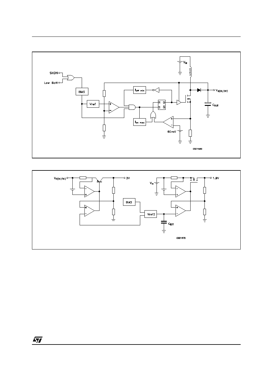
DC/DC CONVERTER BLOCK DIAGRAM
LINEAR VREG BLOCK DIAGRAM