 | –≠–ª–µ–∫—Ç—Ä–æ–Ω–Ω—ã–π –∫–æ–º–ø–æ–Ω–µ–Ω—Ç: 74AC16541 | –°–∫–∞—á–∞—Ç—å:  PDF PDF  ZIP ZIP |
1/9
February 2003
s
HIGH SPEED:
t
PD
= 4.5 ns (TYP.) at V
CC
= 5V
s
LOW POWER DISSIPATION:
I
CC
= 8
µ
A (MAX.) at T
A
=25∞C
s
HIGH NOISE IMMUNITY:
V
NIH
= V
NIL
= 28% V
CC
(MIN.)
s
POWER DOWN PROTECTION ON INPUTS
s
SYMMETRICAL OUTPUT IMPEDANCE:
|I
OH
| = I
OL
= 24 mA (MIN)
s
BALANCED PROPAGATION DELAYS:
t
PLH
t
PHL
s
OPERATING VOLTAGE RANGE:
V
CC
(OPR) = 2V to 6V
s
PIN AND FUNCTION COMPATIBLE WITH
74 SERIES 16541
s
IMPROVED LATCH-UP IMMUNITY
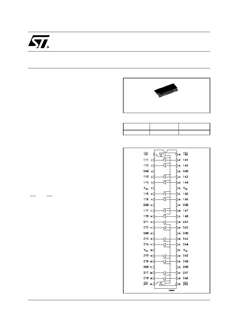
DESCRIPTION
The 74AC16541 is an advanced high-speed
CMOS 16-BIT BUS BUFFER (3-STATE) fabricat-
ed with sub-micron silicon gate and double-layer
metal wiring C
2
MOS tecnology.
This is composed of two 8-bit sections with
separate output-enable signals. For either 8-bit
buffers section, the
3 STATE control gate
operates as a two input AND such that if either
nG1 and nG2 are high, all outputs are in the high
impedence state.
74AC16541
16-BIT BUS BUFFER
WITH 3-STATE OUTPUTS (NON INVERTED)
ORDER CODES
PACKAGE
TUBE
T & R
TSSOP
74AC16541TTR
TSSOP
PIN CONNECTION

74AC16541
2/9
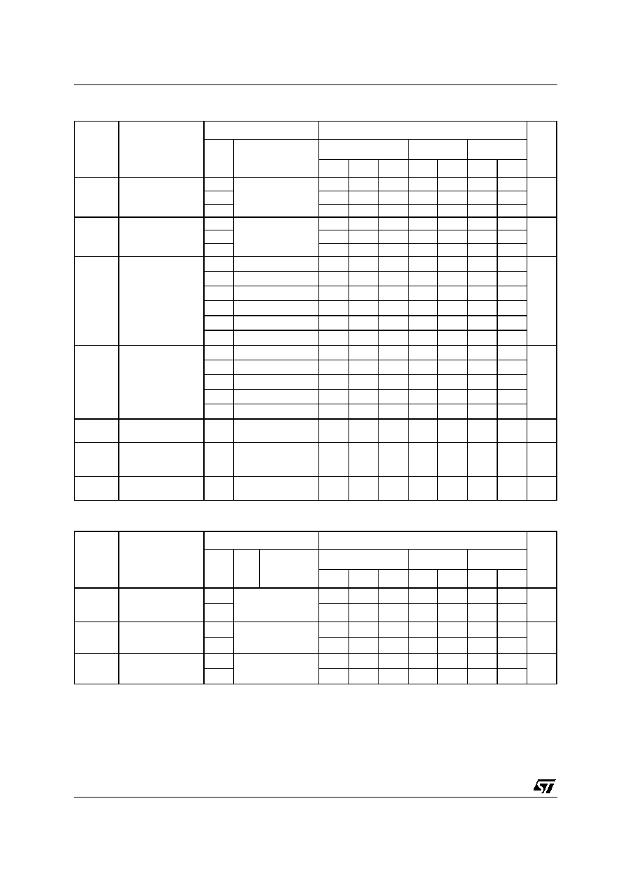
INPUT AND OUTPUT EQUIVALENT CIRCUIT
PIN DESCRIPTION
TRUTH TABLE
X : Don't Care
Z : High Impedance
IEC LOGIC SYMBOLS
PIN No
SYMBOL
NAME AND FUNCTION
1, 48
1G1, 1G2
Output Enable Inputs
2, 3, 5, 6, 8, 9,
11, 12
1Y1 to 1Y8 Data Outputs
13, 14, 16, 17,
19, 20, 22, 23
2Y1 to 2Y8 Data Outputs
24, 25
2G1, 2G2
Output Enable Inputs
36, 35, 33, 32,
30, 29, 27, 26
2A1 to 2A8 Data Outputs
47, 46, 44, 43,
41, 40, 38, 37
1A1 to 1A8 Data Outputs
4, 10, 15, 21,
28, 34, 39, 45
GND
Ground (0V)
7, 18, 31, 42
V
CC
Positive Supply Voltage
INPUTS
OUTPUT
G1
G2
An
Yn
H
X
X
Z
X
H
X
Z
L
L
H
H
L
L
L
L

74AC16541
3/9
ABSOLUTE MAXIMUM RATINGS
Absolute Maximum Ratings are those values beyond which damage to the device may occur. Functional operation under these conditions is
not implied
RECOMMENDED OPERATING CONDITIONS
1) V
IN
from 30% to 70% of V
CC
Symbol
Parameter
Value
Unit
V
CC
Supply Voltage
-0.5 to +7.0
V
V
I
DC Input Voltage
-0.5 to +7.0
V
V
O
DC Output Voltage
-0.5 to V
CC
+ 0.5
V
I
IK
DC Input Diode Current
±
20
mA
I
OK
DC Output Diode Current
±
50
mA
I
O
DC Output Current
±
50
mA
I
CC
or I
GND
DC V
CC
or Ground Current
±
400
mA
T
stg
Storage Temperature
-65 to +150
∞C
T
L
Lead Temperature (10 sec)
300
∞C
Symbol
Parameter
Value
Unit
V
CC
Supply Voltage
2 to 6
V
V
I
Input Voltage
0 to V
CC
V
V
O
Output Voltage
0 to V
CC
V
T
op
Operating Temperature
-55 to 125
∞C
dt/dv
Input Rise and Fall Time (note 1) V
CC
= 3.0, 4.5 or 5.5
0 to 8
ns/V
74AC16541
4/9
DC SPECIFICATIONS
AC ELECTRICAL CHARACTERISTICS ( C
L
= 50 pF, R
L
= 500
, Input t
r
= t
f
= 3ns)
(*) Voltage range is 3.3V
±
0.3V
(**) Voltage range is 5.0V
±
0.5V
Symbol
Parameter
Test Condition
Value
Unit
V
CC
(V)
T
A
= 25 ∞C
-40 to 85∞C
-55 to 125∞C
Min.
Typ.
Max.
Min.
Max.
Min.
Max.
V
IH
High Level Input
Voltage
3.0
V
O
= 0.1 V or
V
CC
-0.1V
2.1
1.5
2.1
2.1
V
4.5
3.15
2.25
3.15
3.15
5.5
3.85
2.75
3.85
3.85
V
IL
Low Level Input
Voltage
3.0
V
O
= 0.1 V or
V
CC
-0.1V
1.5
0.9
0.9
0.9
V
4.5
2.25
1.35
1.35
1.35
5.5
2.75
1.65
1.65
1.65
V
OH
High Level Output
Voltage
3.0
I
O
=-50
µ
A
2.9
2.99
2.9
2.9
V
4.5
I
O
=-50
µ
A
4.4
4.49
4.4
4.4
5.5
I
O
=-50
µ
A
5.4
5.49
5.4
5.4
3.0
I
O
=-12 mA
2.56
2.46
2.46
4.5
I
O
=-24 mA
3.86
3.76
3.76
5.5
I
O
=-24 mA
4.86
4.76
4.76
V
OL
Low Level Output
Voltage
3.0
I
O
=50
µ
A
0.002
0.1
0.1
0.1
V
4.5
I
O
=50
µ
A
0.001
0.1
0.1
0.1
5.5
I
O
=50
µ
A
0.001
0.1
0.1
0.1
3.0
I
O
=12 mA
0.36
0.44
0.44
4.5
I
O
=24 mA
0.36
0.44
0.44
I
I
Input Leakage
Current
5.5
V
I
= V
CC
or GND
±
0.1
±
1
±
1
µ
A
I
OZ
High Impedance
Output Leakage
Current
5.5
V
I
= V
IH
or V
IL
V
O
= V
CC
or GND
±
0.5
±
5
±
5
µ
A
I
CC
Quiescent Supply
Current
5.5
V
I
= V
CC
or GND
8
80
80
µ
A
Symbol
Parameter
Test Condition
Value
Unit
V
CC
(V)
C
L
(pF)
T
A
= 25∞C
-40 to 85∞C
-55 to 125∞C
Min.
Typ.
Max.
Min.
Max.
Min.
Max.
t
PLH
t
PHL
Propagation Delay
Time
A to Y
3.3
(*)
6.3
7.5
9.5
9.5
ns
5.0
(**)
4.5
7.0
9.0
9.0
t
PZL
t
PZH
Output Enable
Time
3.3
(*)
8.5
10.0
12.0
12.0
ns
5.0
(**)
5.5
7.0
9.0
9.0
t
PLZ
t
PHZ
Output Disable
Time
3.3
(*)
7.5
9.0
11.5
11.5
ns
5.0
(**)
6.0
8.0
11.0
11.0
74AC16541
5/9
CAPACITIVE CHARACTERISTICS
1) C
PD
is defined as the value of the IC's internal equivalent capacitance which is calculated from the operating current consumption without
load. (Refer to Test Circuit). Average operating current can be obtained by the following equation. I
CC(opr)
= C
PD
x V
CC
x f
IN
+ I
CC
/ 16
TEST CIRCUIT
C
L
= 50 pF or equivalent (includes jig and probe capacitance)
R
L
= R1 = 500
or equivalent
R
T
= Z
OUT
of pulse generator (typically 50
)
Symbol
Parameter
Test Condition
Value
Unit
V
CC
(V)
T
A
= 25∞C
-40 to 85∞C
-55 to 125∞C
Min.
Typ.
Max.
Min.
Max.
Min.
Max.
C
IN
Input Capacitance
7
10
10
10
pF
C
OUT
Output
Capacitance
14
pF
C
PD
Power Dissipation
Capacitance
(note 1)
5.0
f
IN
= 10MHz
25
pF
TEST
SWITCH
t
PLH
, t
PHL
Open
t
PZL
, t
PLZ
V
CC
t
PZH
, t
PHZ
GND