 | –≠–ª–µ–∫—Ç—Ä–æ–Ω–Ω—ã–π –∫–æ–º–ø–æ–Ω–µ–Ω—Ç: 74AC257 | –°–∫–∞—á–∞—Ç—å:  PDF PDF  ZIP ZIP |
1/11
April 2001
s
HIGH SPEED: t
PD
= 4.5ns (TYP.) at V
CC
= 5V
s
LOW POWER DISSIPATION:
I
CC
= 4
µ
A(MAX.) at T
A
=25∞C
s
HIGH NOISE IMMUNITY:
V
NIH
= V
NIL
= 28 % V
CC
(MIN.)
s
50
TRANSMISSION LINE DRIVING
CAPABILITY
s
SYMMETRICAL OUTPUT IMPEDANCE:
|I
OH
| = I
OL
= 24mA (MIN)
s
BALANCED PROPAGATION DELAYS:
t
PLH
t
PHL
s
OPERATING VOLTAGE RANGE:
V
CC
(OPR) = 2V to 6V
s
PIN AND FUNCTION COMPATIBLE WITH
74 SERIES 257
s
IMPROVED LATCH-UP IMMUNITY
DESCRIPTION
The 74AC257 is an advanced high-speed CMOS
QUAD 2-CHANNEL MULTIPLEXER (3-STATE)
fabricated with sub-micron silicon gate and
double-layer metal wiring C
2
MOS tecnology.
It is composed of four independent 2-channel
multiplexer with common SELECT and ENABLE
(OE) inputs. It is a non-inverting multiplexer. When
the OE input is held HIGH,all the output become in
high impedance state. If SELECT input is held
LOW, "A" data is selected, when SELECT input is
held HIGH, "B" data is chosen.
All inputs and outputs are equipped with
protection circuits against static discharge, giving
them 2KV ESD immunity and transient excess
voltage.
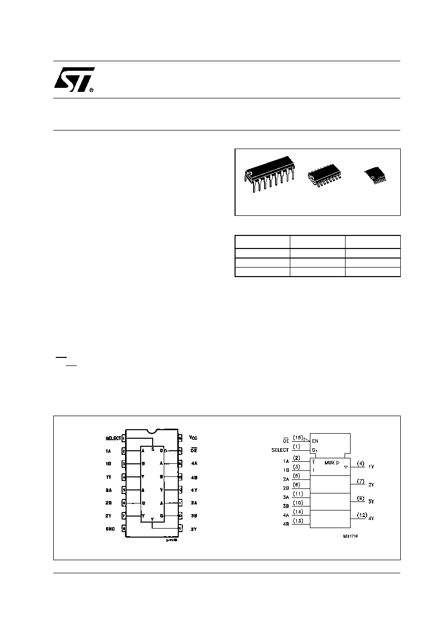
74AC257
QUAD 2 CHANNEL MULTIPLEXER (3-STATE)
PIN CONNECTION AND IEC LOGIC SYMBOLS
ORDER CODES
PACKAGE
TUBE
T & R
DIP
74AC257B
SOP
74AC257M
74AC257MTR
TSSOP
74AC257TTR
TSSOP
DIP
SOP
74AC257
2/11
INPUT AND OUTPUT EQUIVALENT CIRCUIT
PIN DESCRIPTION
TRUTH TABLE
X : Don't Care
Z : High Impedance
LOGIC DIAGRAM
This logic diagram has not be used to estimate propagation delays
PIN No
SYMBOL
NAME AND FUNCTION
1
SELECT
Common Data Select
Inputs
2, 5, 11, 14
1A to 4A
Data Inputs From Source
A
3, 6, 10, 13
1B to 4B
Data Inputs From Source
B
4, 7, 9, 12
1Y to 4Y
Multiplexer Outputs
15
OE
3 State Output Enable
Inputs (Active LOW)
8
GND
Ground (0V)
16
V
CC
Positive Supply Voltage
INPUTS
OUTPUT
OE
SELECT
A
B
Y
H
X
X
X
L
L
L
L
X
L
L
L
H
X
H
L
H
X
L
L
L
H
X
H
H
74AC257
3/11
ABSOLUTE MAXIMUM RATINGS
Absolute Maximum Ratings are those values beyond which damage to the device may occur. Functional operation under these conditions is
not implied.
RECOMMENDED OPERATING CONDITIONS
1) V
IN
from 30% to 70% of V
CC
Symbol
Parameter
Value
Unit
V
CC
Supply Voltage
-0.5 to +7
V
V
I
DC Input Voltage
-0.5 to V
CC
+ 0.5
V
V
O
DC Output Voltage
-0.5 to V
CC
+ 0.5
V
I
IK
DC Input Diode Current
±
20
mA
I
OK
DC Output Diode Current
±
20
mA
I
O
DC Output Current
±
50
mA
I
CC
or I
GND
DC V
CC
or Ground Current
±
200
mA
T
stg
Storage Temperature
-65 to +150
∞C
T
L
Lead Temperature (10 sec)
300
∞C
Symbol
Parameter
Value
Unit
V
CC
Supply Voltage
2 to 6
V
V
I
Input Voltage
0 to V
CC
V
V
O
Output Voltage
0 to V
CC
V
T
op
Operating Temperature
-55 to 125
∞C
dt/dv
Input Rise and Fall Time V
CC
= 3.0, 4.5 or 5.5V (note 1)
8
ns/V
74AC257
4/11
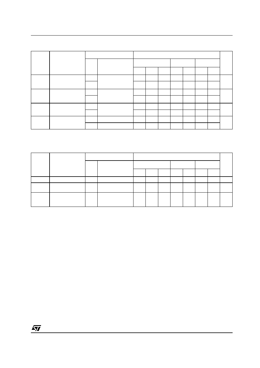
DC SPECIFICATIONS
1) Maximum test duration 2ms, one output loaded at time
2) Incident wave switching is guaranteed on transmission lines with impedances as low as 50
Symbol
Parameter
Test Condition
Value
Unit
V
CC
(V)
T
A
= 25∞C
-40 to 85∞C
-55 to 125∞C
Min.
Typ.
Max.
Min.
Max.
Min.
Max.
V
IH
High Level Input
Voltage
3.0
V
O
= 0.1 V or
V
CC
-0.1V
2.1
1.5
2.1
2.1
V
4.5
3.15
2.25
3.15
3.15
5.5
3.85
2.75
3.85
3.85
V
IL
Low Level Input
Voltage
3.0
V
O
= 0.1 V or
V
CC
-0.1V
1.5
0.9
0.9
0.9
V
4.5
2.25
1.35
1.35
1.35
5.5
2.75
1.65
1.65
1.65
V
OH
High Level Output
Voltage
3.0
I
O
=-50
µ
A
2.9
2.99
2.9
2.9
V
4.5
I
O
=-50
µ
A
4.4
4.49
4.4
4.4
5.5
I
O
=-50
µ
A
5.4
5.49
5.4
5.4
3.0
I
O
=-12 mA
2.56
2.46
2.4
4.5
I
O
=-24 mA
3.86
3.76
3.7
5.5
I
O
=-24 mA
4.86
4.76
4.7
V
OL
Low Level Output
Voltage
3.0
I
O
=50
µ
A
0.002
0.1
0.1
0.1
V
4.5
I
O
=50
µ
A
0.001
0.1
0.1
0.1
5.5
I
O
=50
µ
A
0.001
0.1
0.1
0.1
3.0
I
O
=12 mA
0.36
0.44
0.5
4.5
I
O
=24 mA
0.36
0.44
0.5
5.5
I
O
=24 mA
0.36
0.44
0.5
I
I
Input Leakage
Current
5.5
V
I
= V
CC
or GND
±
0.1
±
1
±
1
µ
A
Ioz
High Impedance
Output Leakage
Current
5.5
V
I
= V
IH
or V
IL
V
O
= V
CC
or GND
±
0.5
±
5
±
10
µ
A
I
CC
Quiescent Supply
Current
5.5
V
I
= V
CC
or GND
4
40
80
µ
A
I
OLD
Dynamic Output
Current (note 1, 2)
5.5
V
OLD
= 1.65 V max
75
50
mA
I
OHD
V
OHD
= 3.85 V min
-75
-50
mA
74AC257
5/11
AC ELECTRICAL CHARACTERISTICS (C
L
= 50 pF, R
L
= 500
, Input t
r
= t
f
= 3ns)
(*) Voltage range is 3.3V
±
0.3V
(**) Voltage range is 5.0V
±
0.5V
CAPACITIVE CHARACTERISTICS
1) C
PD
is defined as the value of the IC's internal equivalent capacitance which is calculated from the operating current consumption without
load. (Refer to Test Circuit). Average operating current can be obtained by the following equation. I
CC(opr)
= C
PD
x V
CC
x f
IN
+ I
CC
/4 (per circuit)
Symbol
Parameter
Test Condition
Value
Unit
V
CC
(V)
T
A
= 25∞C
-40 to 85∞C
-55 to 125∞C
Min.
Typ.
Max.
Min.
Max.
Min.
Max.
t
PLH
t
PHL
Propagation Delay
Time
A, B to Y
3.3
(*)
1.5
5.5
8.5
1.5
9.0
1.5
9.0
ns
5.0
(**)
1.5
4.5
6.0
1.5
7.0
1.5
7.0
t
PLH
t
PHL
Propagation Delay
Time
SELECT to Y
3.3
(*)
1.5
7.0
10.5
1.5
11.5
1.5
11.5
ns
5.0
(**)
1.5
5.5
7.5
1.5
8.5
1.5
8.5
t
PZL
t
PZH
Output Enable
Time
3.3
(*)
1.5
5.5
9.0
1.5
100
1.5
100
ns
5.0
(**)
1.5
4.5
7.5
1.5
8.5
1.5
8.5
t
PLZ
t
PHZ
Output Disable
Time
3.3
(*)
1.5
7.0
10.0
1.5
11.0
1.5
13.0
ns
5.0
(**)
1.5
5.5
9.0
1.5
10.0
1.5
11.0
Symbol
Parameter
Test Condition
Value
Unit
V
CC
(V)
T
A
= 25∞C
-40 to 85∞C
-55 to 125∞C
Min.
Typ.
Max.
Min.
Max.
Min.
Max.
C
IN
Input Capacitance
5.0
5
pF
C
OUT
Output
Capacitance
5.0
8
pF
C
PD
Power Dissipation
Capacitance (note
1)
5.0
f
IN
= 10MHz
20
pF