
74ACT273
OCTAL D-TYPE FLIP FLOP WITH CLEAR
PRELIMINARY DATA
Æ
May 1999
s
HIGH SPEED:
f
MAX
= 190 MHz ns (TYP.) at V
CC
= 5V
s
LOW POWER DISSIPATION:
I
CC
= 8
µ
A (MAX.) at T
A
= 25
o
C
s
COMPATIBLE WITH TTL OUTPUTS
V
IH
= 2V (MIN), V
IL
= 0.8V (MAX)
s
50
TRANSMISSION LINE DRIVING
CAPABILITY
s
SYMMETRICAL OUTPUT IMPEDANCE:
|I
OH
| = I
OL
= 24 mA (MIN)
s
BALANCED PROPAGATION DELAYS:
t
PLH
t
PHL
s
OPERATING VOLTAGE RANGE:
V
CC
(OPR) = 4.5V to 5.5V
s
PIN AND FUNCTION COMPATIBLE WITH
74 SERIES 273
s
IMPROVED LATCH-UP IMMUNITY
DESCRIPTION
The ACT273 is a high-speed CMOS OCTAL
D-TYPE FLIP FLOP WITH
CLEAR fabricated
with sub-micron silicon gate and double-layer
metal wiring C
2
MOS technology. It is ideal for low
power
applications
mantaining
high
speed
operation similar to equivalent Bipolar Schottky
TTL.
Information signals applied to D inputs are
transfered to the Q output on the positive going
edge of the clock pulse.
When the CLEAR input is held low, the Q outputs
are held low independentely of the other inputs .
The device is designed to interface directly High
Speed CMOS systems with TTL, NMOS and
CMOS output voltage levels.
All inputs
and
outputs are
equipped with
protection circuits against static discharge, giving
them 2KV ESD immunity and transient excess
voltage.
PIN CONNECTION AND IEC LOGIC SYMBOLS
M
(Micro Package)
B
(Plastic Package)
T
(TSSOP Package)
ORDER CODES :
74ACT273B
74ACT273M
74ACT273T
1/11

INPUT AND OUTPUT EQUIVALENT CIRCUIT
LOGIC DIAGRAMS
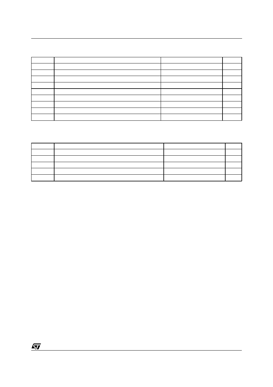
PIN DESCRIPTION
PIN No
SYMBOL
NAME AND FUNCT ION
1
CLEAR
Asyncronous Master
Reset (Active LOW)
2, 5, 6, 9, 12,
15, 16, 19
Q0 to Q7
Flip-Flop Outpus
3, 4, 7, 8, 13,
14, 17, 18
D0 to D7
Data Inputs
11
CLOCK
Clock Input
(LOW-to-HIGH, Edge-
Triggered)
10
GND
Ground (0V)
20
V
CC
Positive Supply Voltage
TRUTH TABLE
I NPUTS
OUT PUT S
F UNCTIO N
CL EAR
D
CLO CK
Q
L
X
X
L
CLEAR
H
L
L
H
H
H
H
X
Q
n
NO CHANGE
X:Don't Care
Thislogic diagram has notbe used to esimate propagation delays
74ACT273
2/11
ABSOLUTE MAXIMUM RATINGS
Symbol
Parameter
Val ue
Unit
V
CC
Supply Voltage
-0.5 to +7
V
V
I
DC Input Voltage
-0.5 to V
CC
+ 0.5
V
V
O
DC Output Voltage
-0.5 to V
CC
+ 0.5
V
I
IK
DC Input Diode Current
±
20
mA
I
OK
DC Output Diode Current
±
20
mA
I
O
DC Output Current
±
50
mA
I
CC
orI
GND
DC V
CC
or Ground Current
±
400
mA
T
stg
Storage Temperature
-65 to +150
o
C
T
L
Lead Temperature (10 sec)
300
o
C
Absolute Maximum Ratings are those values beyond which damage to the device may occur. Functional operation under these condition is not implied.
RECOMMENDED OPERATING CONDITIONS
Symbol
Parameter
Value
Unit
V
CC
Supply Voltage
4.5 to 5.5
V
V
I
Input Voltage
0 to V
CC
V
V
O
Output Voltage
0 to V
CC
V
T
op
Operating Temperature:
-40 to +85
o
C
dt/dv
Input Rise and Fall Time V
CC
= 4.5 to 5.5V (note 1)
8
ns/V
1) V
IN
from 0.8 V to 2.0 V
74ACT273
3/11

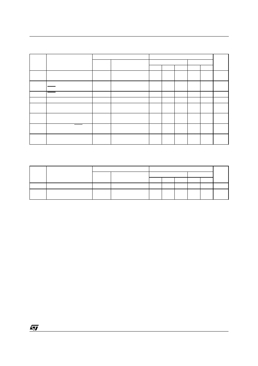
DC SPECIFICATIONS
Symb ol
Parameter
Test Co nditi ons
Valu e
Un it
V
CC
(V)
T
A
= 25
o
C
-40 to 85
o
C
Min.
T yp.
Max.
Mi n.
Max.
V
IH
High Level Input Voltage
4.5
V
O
= 0.1 V or
V
CC
- 0.1 V
2.0
1.5
2.0
V
5.5
2.0
1.5
2.0
V
IL
Low Level Input Voltage
4.5
V
O
= 0.1 V or
V
CC
- 0.1 V
1.5
0.8
0.8
V
5.5
1.5
0.8
0.8
V
OH
High Level Output
Voltage
4.5
V
I
(*)
=
V
IH
or
V
IL
I
O
=-50
µ
A
4.4
4.49
4.4
V
5.5
I
O
=-50
µ
A
5.4
5.49
5.4
4.5
I
O
=-24 mA
3.86
3.76
5.5
I
O
=-24 mA
4.86
4.76
V
OL
Low Level Output
Voltage
4.5
V
I
(*)
=
V
IH
or
V
IL
I
O
=50
µ
A
0.001
0.1
0.1
V
5.5
I
O
=50 mA
0.001
0.1
0.1
4.5
I
O
=24 mA
0.36
0.44
5.5
I
O
=24 mA
0.36
0.44
I
I
Input Leakage Current
5.5
V
I
= V
CC
orGND
±
0.1
±
1
µ
A
I
CCT
Max I
CC
/Input
5.5
V
I
= V
CC
-2.1V
0.6
1.5
mA
I
CC
Quiescent Supply
Current
5.5
V
I
= V
CC
orGND
4
40
µ
A
I
OLD
Dynamic Output Current
(note 1, 2)
5.5
V
OLD
= 1.65 V max
75
mA
I
OHD
V
OHD
= 3.85 V min
-75
mA
1) Maximum test duration 2ms, one output loaded attime
2) Incident wave switching is guaranteed on transmission lines with impedances as low as 50
.
74ACT273
4/11
AC ELECTRICAL CHARACTERISTICS (C
L
= 50 pF, R
L
= 500
, Input t
r
= t
f
=3 ns)
Symb ol
Parameter
T est Con ditio n
Valu e
Un it
V
CC
(V)
T
A
= 25
o
C
-40 to 85
o
C
Min.
T yp.
Max.
Mi n.
Max.
t
PLH
t
PHL
Propagation Delay Time
CK to Q
5.0
(*)
1.5
6.5
8.5
1.5
9.0
ns
t
PLH
t
PHL
Propagation Delay Time
CLR to Q
5.0
(*)
1.5
7.0
9.0
1.5
9.5
ns
t
wL
CLR pulse Width, LOW
5.0
(*)
1.5
4.0
4.0
ns
t
w
CK pulse Width
5.0
(*)
1.0
4.0
4.0
ns
t
s
Setup Time Q to CK
HIGH or LOW
5.0
(*)
1.0
3.5
3.5
ns
t
h
Hold Time Q to CK
HIGH or LOW
5.0
(*)
-0.5
1.5
1.5
ns
t
REM
Recovery Time CLR to
CK
5.0
(*)
0.5
3.0
3.0
ns
f
MAX
Maximum Clock
Frequency
5.0
(*)
125
190
110
MHz
(*) Voltage range is 5V
±
0.5V
CAPACITIVE CHARACTERISTICS
Symb ol
Parameter
Test Co nditi ons
Valu e
Un it
V
CC
(V)
T
A
= 25
o
C
-40 to 85
o
C
Min.
T yp.
Max.
Mi n.
Max.
C
IN
Input Capacitance
5.0
4
pF
C
PD
Power Dissipation
Capacitance (note 1)
5.0
f
IN
= 10 MHz
32
pF
1) C
PD
isdefined as the value of the IC'sinternal equivalent capacitance which is calculated fromthe operating current consumption without load. (Referto
Test Circuit).Average operting current can be obtained by the following equation. I
CC
(opr) = C
PD
∑
V
CC
∑
f
IN
+ I
CC
/n(per circuit)
74ACT273
5/11