M54/74HC620
M54/74HC623
October 1992
HC620 3 STATE INVERTING HC623 3 STATE NON INVERTING
OCTAL BUS TRANSCEIVER
B1R
(Plastic Package)
ORDER CODES :
M54HCXXXF1R
M74HCXXXM1R
M74HCXXXB1R
M74HCXXXC1R
F1R
(Ceramic Package)
M1R
(Micro Package)
C1R
(Chip Carrier)
PIN CONNECTIONS (top view)
NC =
No Internal
Connection
DESCRIPTION
.
HIGH SPEED
t
PD
= 10 ns (TYP.) AT V
CC
= 5 V
.
LOW POWER DISSIPATION
I
CC
= 4
µ
A (MAX.) AT T
A
= 25
∞
C
.
HIGH NOISE IMMUNITY
V
NIH
= V
NIL
= 28 % V
CC
(MIN.)
.
OUTPUT DRIVE CAPABILITY
15 LSTTL LOADS
.
SYMMETRICAL OUTPUT IMPEDANCE
|I
OH
| = I
OL
= 6 mA (MIN.)
.
BALANCED PROPAGATION DELAYS
t
PLH
= t
PHL
.
WIDE OPERATING VOLTAGE RANGE
V
CC
(OPR) = 2 V to 6 V
.
PIN AND FUNCTION COMPATIBLE
WITH LS620/623
The M54/74HC620/623 are high speed CMOS
OCTAL BUS TRANSCEIVERS fabricated in silicon
gate C
2
MOS technology. They have the same high
speed performance of LSTTL combined with true
CMOS low power consumption.
These octal bus transceivers are designed for asyn-
chronous two-way communication between data
buses. The control function implementation allows
maximum flexibility in timing.
These devices allow data transmission from the A
bus to B bus or from the B to the A bus depending
upon the logic levels at the enable inputs (GBA and
GAB). The enable inputs can be used to disable the
device so that the buses are effectively isolated.
The dual-enable configuration gives these devices
the capability to store data by simultaneous enabling
of GBA and GAB.
Each output reinforces its input in this transceiver
configuration. Thus, when both control inputs are
enabled and all other data sources to the two sets
of bus lines are at high impedance, both sets of bus
lines (16 in all) will remain at their last states. The 8-
bit codes appearing on the two sets of buses will be
identical for the 'HC623 or complementary for the
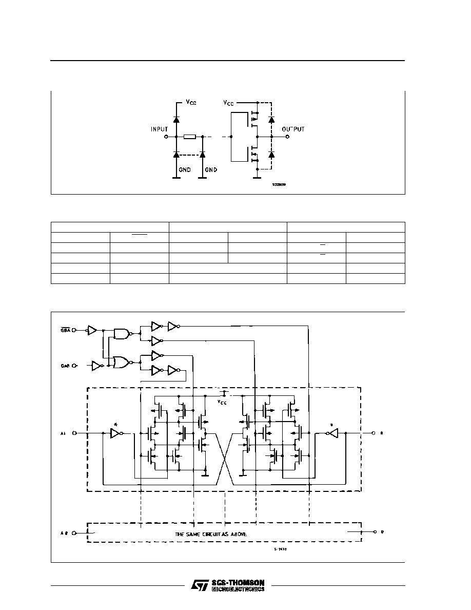
'HC620. All inputs are equipped with protection cir-
cuits against static discharge and transient excess
voltage.
1/11
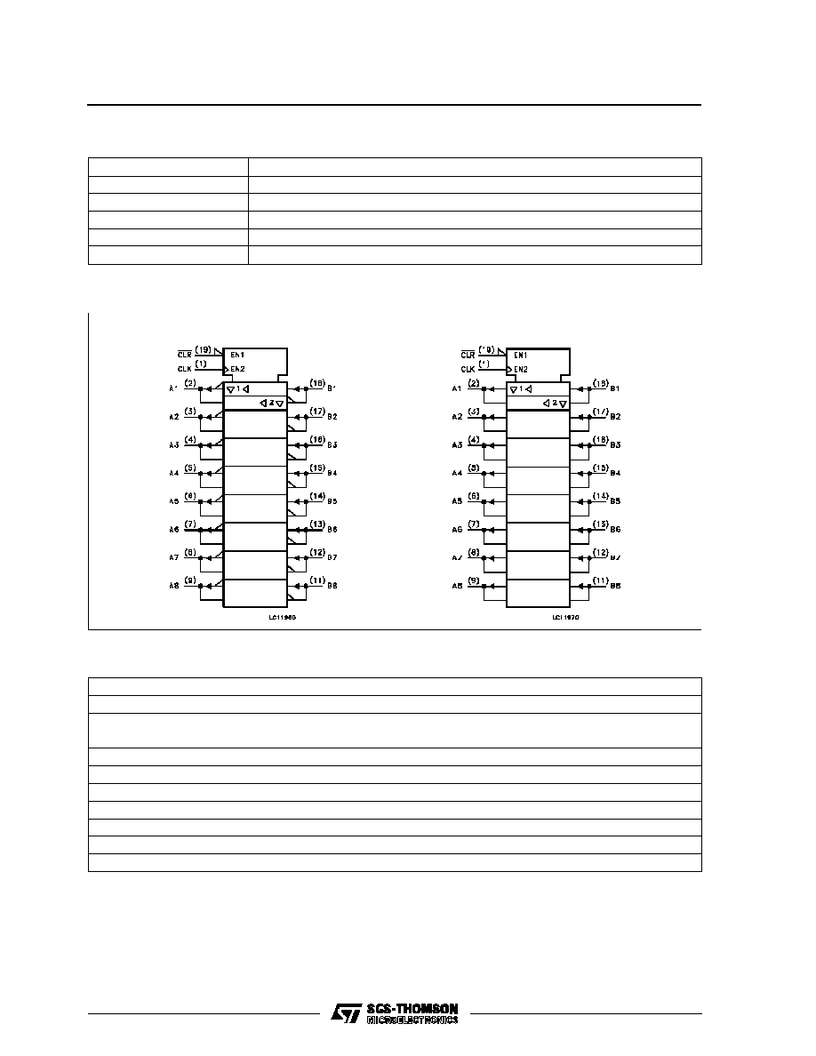
PIN DESCRIPTION
PIN No
SYMBOL
NAME AND FUNCTION
1, 19
GBA , GAB
Direction Controls
2, 3, 4, 5, 6, 7, 8, 9
A1 to A8
Data Inputs/Outputs
11, 12, 13, 14, 15, 16, 17, 18
B1 to B8
Data Inputs/Outputs
10
GND
Ground (0V)
20
V
CC
Positive Supply Voltage
IEC LOGIC SYMBOLS
ABSOLUTE MAXIMUM RATINGS
Symbol
Parameter
Value
Unit
V
CC
Supply Voltage
-0.5 to +7
V
V
I
DC Input Voltage
-0.5 to V
CC
+ 0.5
V
V
O
DC Output Voltage
-0.5 to V
CC
+ 0.5
V
I
IK
DC Input Diode Current
±
20
mA
I
OK
DC Output Diode Current
±
20
mA
I
O
DC Output Source Sink Current Per Output Pin
±
35
mA
I
CC
or I
GND
DC V
CC
or Ground Current
±
70
mA
P
D
Power Dissipation
500 (*)
mW
T
stg
Storage Temperature
-65 to +150
o
C
T
L
Lead Temperature (10 sec)
300
o
C
Absolute Maximum Ratings are those values beyond which damage to the device may occur. Functional operation under these condition is not implied.
(*) 500 mW:
65
o
C derate to 300 mW by 10mW/
o
C: 65
o
C to 85
o
C
HC620
HC623
M54/M74HC620/623
3/11

RECOMMENDED OPERATING CONDITIONS
Symbol
Parameter
Value
Unit
V
CC
Supply Voltage
2 to 6
V
V
I
Input Voltage
0 to V
CC
V
V
O
Output Voltage
0 to V
CC
V
T
op
Operating Temperature: M54HC Series
M74HC Series
-55 to +125
-40 to +85
o
C
o
C
t
r
, t
f
Input Rise and Fall Time
V
CC
= 2 V
0 to 1000
ns
V
CC
= 4.5 V
0 to 500
V
CC
= 6 V
0 to 400
DC SPECIFICATIONS
Symbol
Parameter
Test Conditions
Value
Unit
V
CC
(V)
T
A
= 25
o
C
54HC and 74HC
-40 to 85
o
C
74HC
-55 to 125
o
C
54HC
Min.
Typ.
Max.
Min.
Max.
Min.
Max.
V
IH
High Level Input
Voltage
2.0
1.5
1.5
1.5
V
4.5
3.15
3.15
3.15
6.0
4.2
4.2
4.2
V
IL
Low Level Input
Voltage
2.0
0.5
0.5
0.5
V
4.5
1.35
1.35
1.35
6.0
1.8
1.8
1.8
V
OH
High Level
Output Voltage
2.0
V
I
=
V
IH
or
V
IL
I
O
=-20
µ
A
1.9
2.0
1.9
1.9
V
4.5
4.4
4.5
4.4
4.4
6.0
5.9
6.0
5.9
5.9
4.5
I
O
=-6.0 mA
4.18
4.31
4.13
4.10
6.0
I
O
=-7.8 mA
5.68
5.8
5.63
5.60
V
OL
Low Level Output
Voltage
2.0
V
I
=
V
IH
or
V
IL
I
O
= 20
µ
A
0.0
0.1
0.1
0.1
V
4.5
0.0
0.1
0.1
0.1
6.0
0.0
0.1
0.1
0.1
4.5
I
O
= 6.0 mA
0.17
0.26
0.33
0.40
6.0
I
O
= 7.8 mA
0.18
0.26
0.33
0.40
I
I
Input Leakage
Current
6.0
V
I
= V
CC
or GND
±
0.1
±
1
±
1
µ
A
I
OZ
3 State Output
Off State Current
6.0
V
I
= V
IH
or V
IL
V
O
= V
CC
or GND
±
0.5
±
5
±
10
µ
A
I
CC
Quiescent Supply
Current
6.0
V
I
= V
CC
or GND
4
40
80
µ
A
M54/M74HC620/623
4/11

AC ELECTRICAL CHARACTERISTICS (C
L
= 50 pF, Input t
r
= t
f
= 6 ns)
Symbol
Parameter
Test Conditions
Value
Unit
V
CC
(V)
C
L
(pF)
T
A
= 25
o
C
54HC and 74HC
-40 to 85
o
C
74HC
-55 to 125
o
C
54HC
Min.
Typ.
Max.
Min.
Max.
Min.
Max.
t
TLH
t
THL
Output Transition
Time
2.0
50
25
60
75
90
ns
4.5
7
12
15
18
6.0
6
10
13
15
t
PLH
t
PHL
Propagation
Delay Time
(for HC620)
2.0
50
41
100
125
150
ns
4.5
12
20
25
30
6.0
10
17
21
26
2.0
150
55
130
165
195
ns
4.5
16
26
33
39
6.0
14
22
28
33
t
PLH
t
PHL
Propagation
Delay Time
(for HC623)
2.0
50
38
85
105
130
ns
4.5
12
17
21
26
6.0
10
14
18
22
2.0
150
51
130
165
195
ns
4.5
16
26
33
39
6.0
14
22
28
33
t
PZL
t
PZH
Output Enable
Time
2.0
50
R
L
= 1 K
57
150
190
225
ns
4.5
19
30
38
45
6.0
16
26
32
38
2.0
150
R
L
= 1 K
69
180
225
270
ns
4.5
23
36
45
54
0
20
31
38
46
t
PLZ
t
PHZ
Output Disable
Time
2.0
50
R
L
= 1 K
43
125
155
190
ns
4.5
18
25
31
38
6.0
15
21
26
32
C
IN
Input Capacitance
5
10
10
10
pF
C
PD
(*)
Power Dissipation
Capacitance
for HC620
for HC623
32
34
pF
C
PD
is defined as the value of the IC's internal equivalent capacitance which is calculated from the operating current consumption without load. (Refer
to Test Circuit). Average operting current can be obtained by the following equation. I
CC
(opr) = C
PD
∑
V
CC
∑
f
IN
+ I
CC
M54/M74HC620/623
5/11