 | –≠–ª–µ–∫—Ç—Ä–æ–Ω–Ω—ã–π –∫–æ–º–ø–æ–Ω–µ–Ω—Ç: B180N55 | –°–∫–∞—á–∞—Ç—å:  PDF PDF  ZIP ZIP |
TARGET SPECIFICATION
Rev 1
January 2006
1/11
11
This is a preliminary information on a new product foreseen to be developed. Details are subject to change without notice
STB180N55
STP180N55
N-CHANNEL 55V - 2.9m
- 120A - D≤PAK - TO-220
MDmeshTM Low Voltage Power MOSFET
General features
ULTRA LOW ON-RESISTANCE
100% AVALANCHE TESTED
Description
This N-Channel enhancement mode MOSFET is
the latest refinement of STMicroelectronic unique
"Single Feature SizeTM" strip-based process with
less critical aligment steps and therefore a
remarkable manufacturing reproducibility. The
resulting transistor shows extremely high packing
density for low on-resistance, rugged avalanche
characteristics and low gate charge
.
Applications
HIGH CURRENT SWITCHING APPLICATION
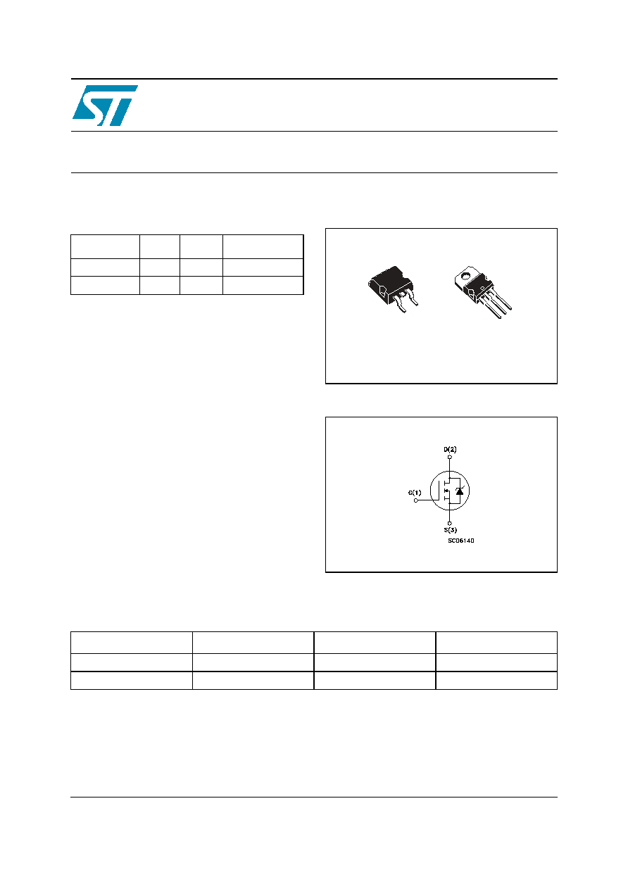
Order codes
Internal schematic diagram
Type
V
DSS
R
DS(on)
I
D
STB180N55
55V
3.5m
120A (
Note
1)
STP180N55
55V
3.8m
120A (
Note
1)
1
3
D≤PAK
1
2
3
TO-220
Sales Type
Marking
Package
Packaging
STB180N55
B180N55
D≤PAK
TAPE & REEL
STP180N55
P180N55
TO-220
TUBE
www.st.com

1 Electrical ratings
STP180N55 - STB180N55
2/11
1 Electrical
ratings
Table 1.
Absolute maximum ratings
Table 2.
Thermal data
Symbol
Parameter
Value
Unit
V
DS
Drain-source Voltage (V
GS
=0)
55
V
V
GS
Gate-Source Voltage
± 20
V
I
D
Note
1
Drain Current (continuous) at T
C
= 25∞C
120
A
I
D
Note
1
Drain Current (continuous) at T
C
= 100∞C
120
A
I
DM
Note
2
Drain Current (pulsed)
480
A
P
TOT
Total Dissipation at T
C
= 25∞C
315
W
Derating Factor
2.1
W/∞C
dv/dt
Peak Diode Recovery voltage slope
TBD
V/ns
E
AS
Note
4
Single Pulse Avalanche Energy
TBD
mJ
T
j
T
stg
Operating Junction Temperature
Storage Temperature
-55 to 175
∞C
TO-220
D≤PAK
Unit
Rthj-case
Thermal Resistance Junction-case
0.48
∞C/W
Rthj-a
Thermal Resistance Junction-ambient Max
62.5
--
∞C/W
Rthj-pcb
Note
5
Thermal Resistance Junction-ambient Max
--
35
∞C/W
T
l
Maximum Lead Temperature For Soldering
Purpose
300
--
∞C

STP180N55 - STB180N55
2 Electrical characteristics
3/11
2 Electrical
characteristics
(T
CASE
= 25 ∞C unless otherwise specified)
Table 3.
On/off states
Table 4.
Dynamic
Symbol
Parameter
Test Conditions
Min.
Typ.
Max.
Unit
V
(BR)DSS
Drain-Source Breakdown
Voltage
I
D
= 250µA, V
GS
= 0
55
V
I
DSS
Zero Gate Voltage Drain
Current (V
GS
= 0)
V
DS
= Max Rating,
V
DS
= Max Rating,Tc = 125∞C
10
100
µA
µA
I
GSS
Gate Body Leakage Current
(V
DS
= 0)
V
GS
= ±20V
±
200
nA
V
GS(th)
Gate Threshold Voltage
V
DS
= V
GS
, I
D
= 250µA
2
4
V
R
DS(on)
Static Drain-Source On
Resistance
V
GS
= 10V, I
D
= 60A D≤PAK
TO-220
3.5
3.8
m
m
Symbol
Parameter
Test Conditions
Min.
Typ.
Max.
Unit
g
fs
Note
3
Forward Transconductance
V
DS
=15V, I
D
= 60A
TBD
S
C
iss
C
oss
C
rss
Input Capacitance
Output Capacitance
Reverse Transfer Capacitance
V
DS
=25V, f=1 MHz, V
GS
=0
6200
1800
100
pF
pF
pF
Q
g
Q
gs
Q
gd
Total Gate Charge
Gate-Source Charge
Gate-Drain Charge
V
DD
=44V, I
D
= 120A
V
GS
=10V
(see Figure 2)
110
TBD
TBD
TBD
nC
nC
nC

2 Electrical characteristics
STP180N55 - STB180N55
4/11
Table 5.
Switching times
Table 6.
Source drain diode
(1) Current limited by package
(2) Pulse width limited by safe operating area
(3) Pulsed: pulse duration = 300µs, duty cycle 1.5%
(4) Starting Tj=25∞C, Id=60A, Vdd=40V
(5) When mounted o inch≤ FR4 2oz Cu
Symbol
Parameter
Test Conditions
Min.
Typ.
Max.
Unit
t
d(on)
t
r
Turn-on Delay Time
Rise Time
V
DD
=27V, I
D
= 60A,
R
G
=4.7
,
V
GS
=10V
(see Figure 3)
TBD
TBD
ns
ns
t
d(off)
t
f
Off voltage Rise Time
FallTime
V
DD
=27V, I
D
= 60A,
R
G
=4.7
,
V
GS
=10V
(see Figure 3)
TBD
TBD
ns
ns
Symbol
Parameter
Test Conditions
Min.
Typ.
Max.
Unit
I
SD
I
SDM
Note
2
Source-drain Current
Source-drain Current (pulsed)
120
480
A
A
V
SD
Note
3
Forward on Voltage
I
SD
=120A, V
GS
=0
1.5
V
t
rr
Q
rr
I
RRM
Reverse Recovery Time
Reverse Recovery Charge
Reverse Recovery Current
I
SD
=120A, di/dt = 100A/µs,
V
DD
=30V, Tj=150∞C
TBD
TBD
TBD
ns
nC
A
STP180N55 - STB180N55
3 Test circuits
5/11
3 Test
circuits
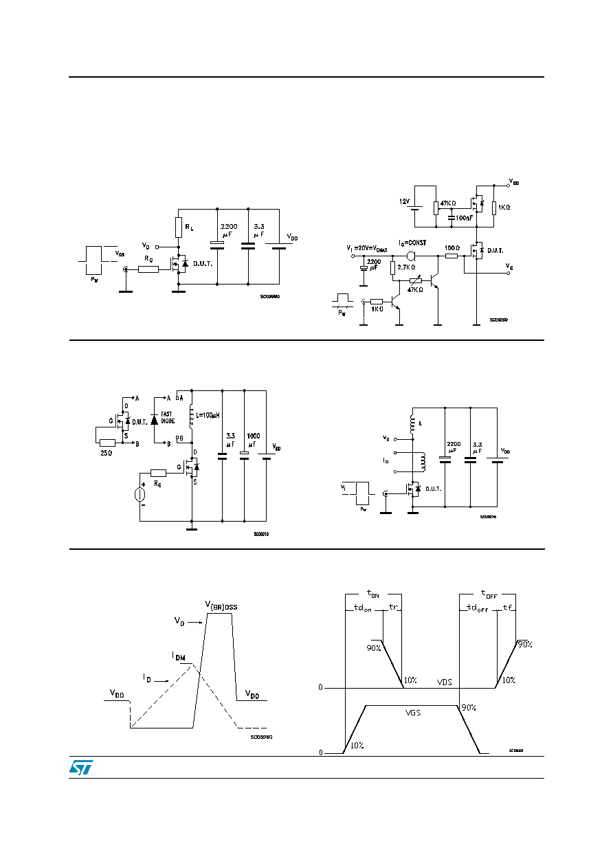
Figure 1.
Switching Times Test Circuit For
Resistive Load
Figure 2.
Gate Charge Test Circuit
Figure 3.
Test Circuit For Indictive Load
Switching and Diode Recovery
Times
Figure 4.
Unclamped Inductive Waveform
Figure 5.
Unclamped Inductive Load Test
Circuit
Figure 6.
Switching Time Waveform