 | –≠–ª–µ–∫—Ç—Ä–æ–Ω–Ω—ã–π –∫–æ–º–ø–æ–Ω–µ–Ω—Ç: BU941PFI | –°–∫–∞—á–∞—Ç—å:  PDF PDF  ZIP ZIP |

BU941/BU941P
BU941PFI
HIGH VOLTAGE IGNITION COIL DRIVER
NPN POWER DARLINGTON
s
NPN DARLINGTON
s
INTEGRATED ANTIPARALLEL
COLLECTOR-EMITTER DIODE
s
VERY RUGGED BIPOLAR TECHNOLOGY
s
HIGH OPERATING JUNCTION
TEMPERATURE
s
WIDE RANGE OF PACKAGES
APPLICATIONS
s
HIGH RUGGEDNESS ELECTRONIC
IGNITIONS
INTERNAL SCHEMATIC DIAGRAM
December 1999
for TO-3
Emitter: pin 2
Base: pin1
Collector: tab
ABSOLUTE MAXIMUM RATINGS
Symbol
Parameter
Val ue
Uni t
BU941
BU941P
BUB941PFI
V
CES
Collect or-Emitter Voltage (V
BE
= 0)
500
V
V
CEO
Collect or-Emitter Voltage (I
B
= 0)
400
V
V
EBO
Emitter-Base Voltage (I
C
= 0)
5
V
I
C
Collect or Current
15
A
I
CM
Collect or Peak Current
30
A
I
B
Base Current
1
A
I
BM
Base Peak Current
5
A
P
t ot
Tot al Dissipation at T
c
= 25
o
C
180
155
65
W
T
stg
Storage T emperat ure
-65 to 200
-65 to 175
-65 t o 175
o
C
T
j
Max. O perating Junction Temperature
200
175
175
o
C
1
2
3
TO-218
ISOWATT218
1
2
3
1
2
TO-3
Æ
1/8

THERMAL DATA
TO-3
TO-218
ISOW AT T218
R
t hj-ca se
Thermal Resistance Junction-case
Max
0.97
0.97
2.3
o
C/W
ELECTRICAL CHARACTERISTICS (T
case
= 25
o
C unless otherwise specified)
Symb ol
Parameter
Test Cond ition s
Mi n.
Typ .
Max.
Un it
I
CES
Collector Cut -of f
Current (V
BE
= 0)
V
CE
= 500 V
V
CE
= 500 V
T
j
= 125
o
C
100
0.5
µ
A
mA
I
CEO
Collector Cut -of f
Current (I
B
= 0)
V
CE
= 450 V
V
CE
= 450 V
T
j
= 125
o
C
100
0.5
µ
A
mA
I
EBO
Emitt er Cut -of f Current
(I
C
= 0)
V
EB
= 5 V
20
mA
V
CEO(sus )
Collector-Emit ter
Sustaining Voltage
(I
B
= 0)
I
C
= 100 mA
L = 10 mH
V
Clamp
= 400 V
(See FIG .4)
400
V
V
CE(sat )
Collector-Emit ter
Saturation Voltage
I
C
= 8 A
I
B
= 100 mA
I
C
= 10 A
I
B
= 250 mA
I
C
= 12 A
I
B
= 300 mA
1.6
1.8
2
V
V
V
V
BE(s at)
Base-Emitt er
Saturation Voltage
I
C
= 8 A
I
B
= 100 mA
I
C
= 10 A
I
B
= 250 mA
I
C
= 12 A
I
B
= 300 mA
2.2
2.5
2.7
V
V
V
h
F E
DC Current Gain
I
C
= 5 A
V
CE
= 10 V
300
V
F
Diode F orward Voltage
I
F
= 10 A
2.5
V
Funct ional T est
(see fig. 1)
V
CC
= 24 V
V
Clam p
= 400 V
L = 7 mH
10
A
t
s
t
f
INDUCTIVE LO AD
St orage Time
Fall Time
(see fig. 3)
V
CC
= 12 V
V
Cl am p
= 300 V
V
BE
= 0
R
BE
= 47
L = 7 mH
I
C
= 7 A
I
B
= 70 mA
15
0.5
µ
s
µ
s
Pulsed: Pulse duration = 300
µ
s, duty cycle 1.5 %
Safe Operating Area
DC Current Gain
BU941 / BU941P / BUB941PFI
2/8

DC Current Gain
Collector-emitter Saturation Voltage
Switching Time Inductive Load (see fig.3)
Collector-emitter Saturation Voltage
Base-emitter Saturation Voltage
BU941 / BU941P / BUB941PFI
3/8

FIGURE 1: Functional Test Circuit
FIGURE 2: Functional Test Waveforms
FIGURE 3: Switching Time Test Circuit
FIGURE 4: Sustaining Voltage Test Circuit
BU941 / BU941P / BUB941PFI
4/8

DIM.
mm
inch
MIN.
TYP.
MAX.
MIN.
TYP.
MAX.
A
11.00
13.10
0.433
0.516
B
0.97
1.15
0.038
0.045
C
1.50
1.65
0.059
0.065
D
8.32
8.92
0.327
0.351
E
19.00
20.00
0.748
0.787
G
10.70
11.10
0.421
0.437
N
16.50
17.20
0.649
0.677
P
25.00
26.00
0.984
1.023
R
4.00
4.09
0.157
0.161
U
38.50
39.30
1.515
1.547
V
30.00
30.30
1.187
1.193
E
B
R
C
D
A
P
G
N
V
U
O
P003F
TO-3 MECHANICAL DATA
BU941 / BU941P / BUB941PFI
5/8

DIM.
mm
inch
MIN.
TYP.
MAX.
MIN.
TYP.
MAX.
A
4.7
4.9
0.185
0.193
C
1.17
1.37
0.046
0.054
D
2.5
0.098
E
0.5
0.78
0.019
0.030
F
1.1
1.3
0.043
0.051
G
10.8
11.1
0.425
0.437
H
14.7
15.2
0.578
0.598
L2
≠
16.2
≠
0.637
L3
18
0.708
L5
3.95
4.15
0.155
0.163
L6
31
1.220
R
≠
12.2
≠
0.480
ÿ
4
4.1
0.157
0.161
R
A
C
D
E
H
F
G
L6
Ø
L3
L2
L5
1
2
3
TO-218 (SOT-93) MECHANICAL DATA
P025A
BU941 / BU941P / BUB941PFI
6/8
DIM.
mm
inch
MIN.
TYP.
MAX.
MIN.
TYP.
MAX.
A
5.35
5.65
0.211
0.222
C
3.30
3.80
0.130
0.150
D
2.90
3.10
0.114
0.122
D1
1.88
2.08
0.074
0.082
E
0.75
0.95
0.030
0.037
F
1.05
1.25
0.041
0.049
F2
1.50
1.70
0.059
0.067
F3
1.90
2.10
0.075
0.083
G
10.80
11.20
0.425
0.441
H
15.80
16.20
0.622
0.638
L
9
0.354
L1
20.80
21.20
0.819
0.835
L2
19.10
19.90
0.752
0.783
L3
22.80
23.60
0.898
0.929
L4
40.50
42.50
1.594
1.673
L5
4.85
5.25
0.191
0.207
L6
20.25
20.75
0.797
0.817
N
2.1
2.3
0.083
0.091
R
4.6
0.181
DIA
3.5
3.7
0.138
0.146
P025C/A
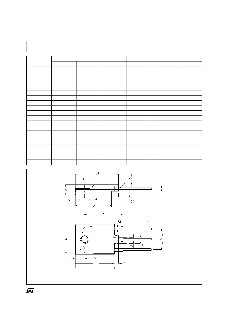
ISOWATT218 MECHANICAL DATA
- Weight : 4.9 g (typ.)
- Maximum Torque (applied to mounting flange) Recommended: 0.8 Nm; Maximum: 1 Nm
- The side of the dissipator must be flat within 80
µ
m
BU941 / BU941P / BUB941PFI
7/8

Information furnished is believed to be accurate and reliable. However, STMicroelectronics assumes no responsibility for the consequences
of use of such information nor for any infringement of patents or other rights of third parties which may result from its use. No license is
granted by implication or otherwise under any patent or patent rights of STMicroelectronics. Specification mentioned in this publication are
subject to change without notice. This publication supersedes and replaces all information previously supplied. STMicroelectronics products
are not authorized for use as critical components in life support devices or systems without express written approval of STMicroelectronics.
The ST logo is a trademark of STMicroelectronics
©
1999 STMicroelectronics ≠ Printed in Italy ≠ All Rights Reserved
STMicroelectronics GROUP OF COMPANIES
Australia - Brazil - China - Finland - France - Germany - Hong Kong - India - Italy - Japan - Malaysia - Malta - Morocco -
Singapore - Spain - Sweden - Switzerland - United Kingdom - U.S.A.
http://www.st.com
.
BU941 / BU941P / BUB941PFI
8/8