
BUH1015HI
HIGH VOLTAGE FAST-SWITCHING
NPN POWER TRANSISTOR
s
STMicroelectronics PREFERRED
SALESTYPE
s
HIGH VOLTAGE CAPABILITY (> 1500 V)
s
VERY HIGH SWITCHING SPEED
s
FULLY INSULATED PACKAGE (U.L.
COMPLIANT) FOR EASY MOUNTING
APPLICATIONS:
s
HORIZONTAL DEFLECTION FOR
HIGH-END COLOUR TV AND 19"
MONITORS
DESCRIPTION
The BUH1015HI is manufactured using
Multiepitaxial Mesa technology for cost-effective
high performance and uses a Hollow Emitter
structure to enhance switching speeds.
The BUH series is designed for use in horizontal
deflection circuits in televisions and monitors.
INTERNAL SCHEMATIC DIAGRAM
April 2002
ABSOLUTE MAXIMUM RATINGS
Symbol
Parameter
Value
Unit
V
CBO
Collector-Base Voltage (I
E
= 0)
1500
V
V
CEO
Collector-Emitter Voltage (I
B
= 0)
700
V
V
EBO
Emitter-Base Voltage (I
C
= 0)
10
V
I
C
Collector Current
14
A
I
CM
Collector Peak Current (t
p
< 5 ms)
18
A
I
B
Base Current
8
A
I
BM
Base Peak Current (t
p
< 5 ms)
11
A
P
tot
Total Dissipation at T
c
= 25
o
C
70
W
V
isol
Insulation Withstand Voltage (RMS) from All
Three Leads to Exernal Heatsink
2500
V
T
stg
Storage Temperature
-65 to 150
o
C
T
j
Max. Operating Junction Temperature
150
o
C
ISOWATT218
1
2
3
�
1/7

THERMAL DATA
R
thj-case
Thermal Resistance Junction-case Max
1.8
o
C/W
ELECTRICAL CHARACTERISTICS (T
case
= 25
o
C unless otherwise specified)
Symbol
Parameter
Test Conditions
Min.
Typ.
Max.
Unit
I
CES
Collector Cut-off
Current (V
BE
= 0)
V
CE
= 1500 V
V
CE
= 1500 V T
j
= 125
o
C
0.2
2
mA
mA
I
EBO
Emitter Cut-off Current
(I
C
= 0)
V
EB
= 5 V
100
�
A
V
CEO(sus)
Collector-Emitter
Sustaining Voltage
(I
B
= 0)
I
C
= 100 mA
700
V
V
EBO
Emitter-Base Voltage
(I
C
= 0)
I
E
= 10 mA
10
V
V
CE(sat)
Collector-Emitter
Saturation Voltage
I
C
= 10 A I
B
= 2 A
1.5
V
V
BE(sat)
Base-Emitter
Saturation Voltage
I
C
= 10 A I
B
= 2 A
1.5
V
h
FE
DC Current Gain
I
C
= 10 A V
CE
= 5 V
I
C
= 10 A V
CE
= 5 V T
j
= 100
o
C
7
5
10
14
t
s
t
f
RESISTIVE LOAD
Storage Time
Fall Time
V
CC
= 400 V I
C
= 10 A
I
B1
= 2 A I
B2
= -6 A
1.5
110
�
s
ns
t
s
t
f
INDUCTIVE LOAD
Storage Time
Fall Time
I
C
= 10 A f = 31250 Hz
I
B1
= 2 A I
B2
= -6 A
V
ceflyback
= 1200 sin
5
10
6
t V
4
220
�
s
ns
t
s
t
f
INDUCTIVE LOAD
Storage Time
Fall Time
I
C
= 6 A f = 64 KHz
I
B1
= 1 A
V
beo ff
= - 2 V
V
ceflyback
= 1100 sin
5
10
6
t V
3.7
200
�
s
ns
Pulsed: Pulse duration = 300
�
s, duty cycle 1.5 %
BUH1015HI
2/7

Safe Operating Area
Derating Curve
Collector Emitter Saturation Voltage
Thermal Impedance
DC Current Gain
Base Emitter Saturation Voltage
BUH1015HI
3/7

Power Losses at 64 KHz
Switching Time Inductive Load at 64KHz
(see figure 2)
In order to saturate the power switch and reduce
conduction losses, adequate direct base current
I
B1
has to be provided for the lowest gain h
FE
at
T
j
= 100
o
C (line scan phase). On the other hand,
negative base current I
B2
must be provided the
transistor to turn off (retrace phase). Most of the
dissipation, especially in the deflection
application, occurs at switch-off so it is essential
to determine the value of I
B2
which minimizes
power losses, fall time t
f
and, consequently, T
j
. A
new set of curves have been defined to give total
power losses, t
s
and t
f
as a function of I
B1
at 64
KHz scanning frequencies for choosing the
optimum drive. The test circuit is illustrated in
figure 1.
The values of L and C are calculated from the
following equations:
1
2
L
(
I
C
)
2
=
1
2
C
(
V
CEfly
)
2
=
2
f
=
1
L
C
Where I
C
= operating collector current, V
CEfly
=
flyback voltage, f= frequency of oscillation during
retrace.
BASE DRIVE INFORMATION
Reverse Biased SOA
BUH1015HI
4/7
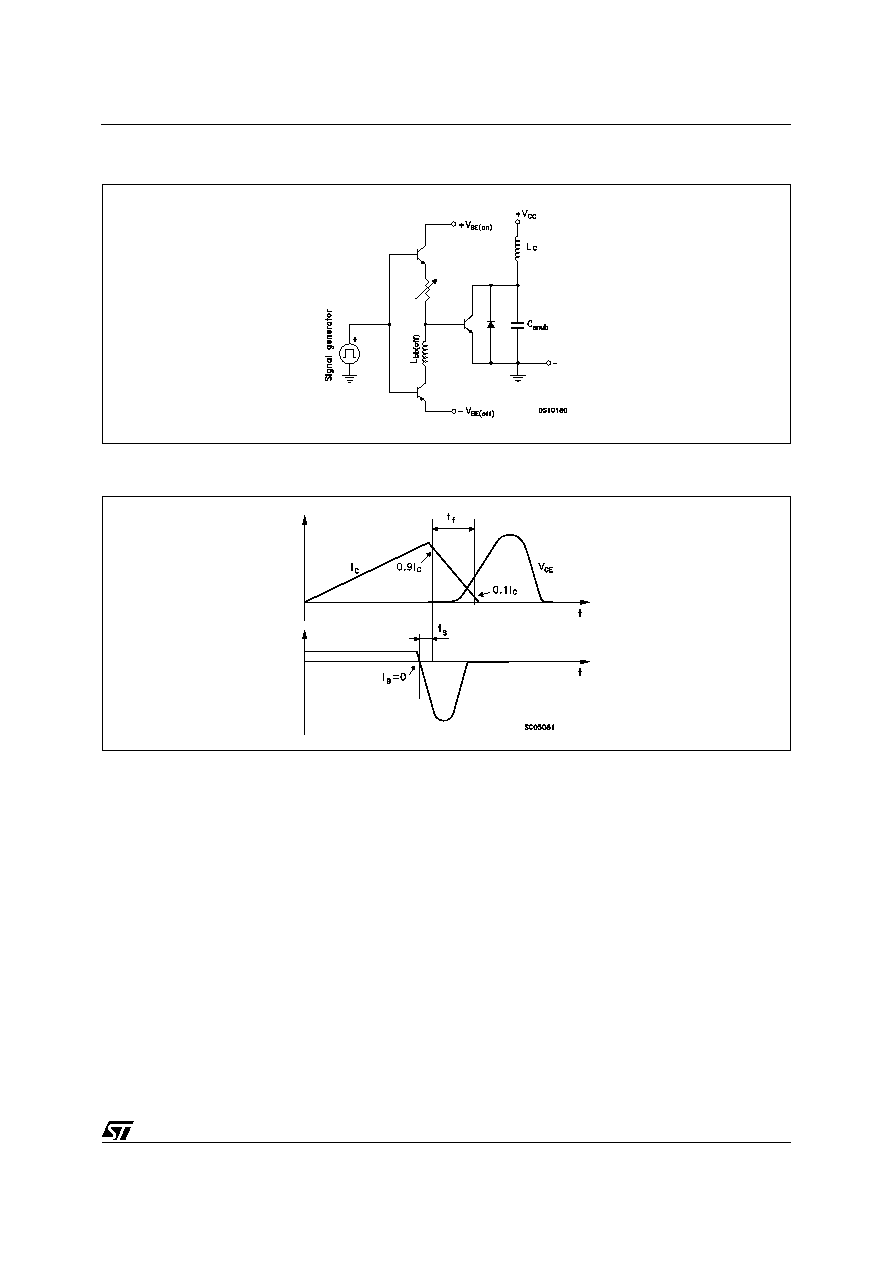
Figure 1: Inductive Load Switching Test Circuit.
Figure 2: Switching Waveforms in a Deflection Circuit
BUH1015HI
5/7