 | –≠–ª–µ–∫—Ç—Ä–æ–Ω–Ω—ã–π –∫–æ–º–ø–æ–Ω–µ–Ω—Ç: BUL382 | –°–∫–∞—á–∞—Ç—å:  PDF PDF  ZIP ZIP |

BUL381
BUL382
HIGH VOLTAGE FAST-SWITCHING
NPN POWER TRANSISTOR
s
STM PREFERRED SALESTYPES
s
HIGH VOLTAGE CAPABILITY
s
MINIMUM LOT-TO-LOT SPREAD FOR
RELIABLE OPERATION
s
VERY HIGH SWITCHING SPEED
s
FULLY CHARACTERISED AT 125
o
C
APPLICATIONS
s
ELECTRONIC BALLASTS FOR
FLUORESCENT LIGHTING
s
SWITCH MODE POWER SUPPLIES
DESCRIPTION
The BUL381 and BUL382 manufactured using
high voltage Multiepitaxial Mesa technology for
cost-effective high performance. They use a
Hollow Emitter structure to enhance switching
speeds.
The BUL series is designed for use in lighting
applications and low cost switch-mode power
supplies.
INTERNAL SCHEMATIC DIAGRAM
June 1998
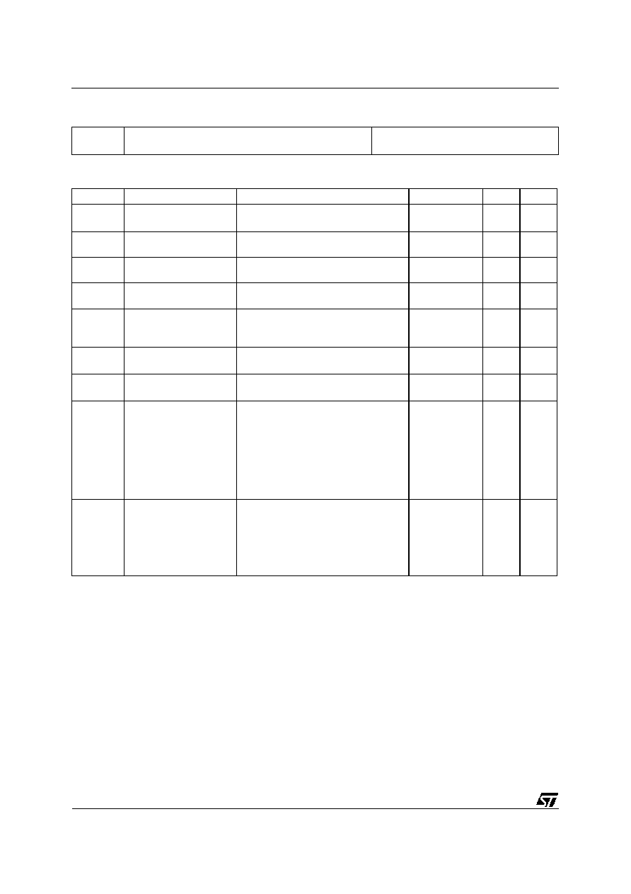
ABSOLUTE MAXIMUM RATINGS
Symbol
Parameter
Val ue
Uni t
V
CES
Collect or-Emitt er Voltage (V
BE
= 0)
800
V
V
CEO
Collect or-Emitt er Voltage (I
B
= 0)
400
V
V
EBO
Emitt er-Base Voltage (I
C
= 0)
9
V
I
C
Collect or Current
5
A
I
CM
Collect or Peak Current (t
p
< 5 ms)
8
A
I
B
Base Current
2
A
I
BM
Base Peak Current (t
p
< 5 ms)
4
A
P
t ot
Total Dissipation at T
c
= 25
o
C
70
W
T
stg
St orage Temperature
-65 to 150
o
C
T
j
Max. Operating Junction Temperature
150
o
C
Æ
1
2
3
TO-220
1/7
THERMAL DATA
R
t hj-ca se
R
t hj- amb
Thermal Resistance Junction-Case
Max
Thermal Resistance Junction-Ambient
Max
1.78
62. 5
o
C/W
o
C/W
ELECTRICAL CHARACTERISTICS (T
case
= 25
o
C unless otherwise specified)
Symb ol
Parameter
Test Cond ition s
Mi n.
Typ .
Max.
Un it
I
CES
Collect or Cut-off
Current (V
BE
= 0)
V
CE
= 800 V
V
CE
= 800 V
T
j
= 125
o
C
100
500
µ
A
µ
A
I
CEO
Collect or Cut-off
Current (I
B
= 0)
V
CE
= 400 V
250
µ
A
V
CEO (sus)
Collect or-Emitter
Sustaining Voltage
I
C
= 100 mA
L = 25 mH
400
V
V
EBO
Emitt er-Base Voltage
(I
C
= 0)
I
E
= 10 mA
9
V
V
CE(sat )
Collect or-Emitter
Saturat ion Voltage
I
C
= 1 A
I
B
= 0.2 A
I
C
= 2 A
I
B
= 0.4 A
I
C
= 3 A
I
B
= 0.8 A
0.5
0.7
1.1
V
V
V
V
BE(s at)
Base-Emitt er
Saturat ion Voltage
I
C
= 1 A
I
B
= 0.2 A
I
C
= 2 A
I
B
= 0.4 A
1.1
1.2
V
V
h
FE
DC Current G ain
I
C
= 2 A
V
CE
= 5 V
I
C
= 10 mA
V
CE
= 5 V
8
10
t
ON
t
s
t
f
RESI STIVE LO AD
Turn-on T ime
St orage Time
Fall T ime
V
CC
= 250 V
I
C
= 2 A
I
B1
= 0.4 A
I
B2
= -0. 4 A
(f or BUL381only)
t
p
= 30
µ
s
1. 4
1
2.2
800
µ
s
µ
s
ns
t
ON
t
s
t
f
RESI STIVE LO AD
Turn-on T ime
St orage Time
Fall T ime
V
CC
= 250 V
I
C
= 2 A
I
B1
= 0.4 A
I
B2
= -0.4 A
(f or BUL382 only)
t
p
= 30
µ
s
1. 7
1
2.5
800
µ
s
µ
s
ns
t
s
t
f
INDUCTIVE LOAD
St orage Time
Fall T ime
I
C
= 2 A
V
CL
= 250 V
I
B1
= 0.4 A
I
B2
= -0. 8 A
L = 200
µ
H
1.7
75
2.6
120
µ
s
ns
t
s
t
f
INDUCTIVE LOAD
St orage Time
Fall T ime
I
C
= 2 A
V
CL
= 250 V
I
B1
= 0.4 A
I
B2
= -0. 8 A
L = 200
µ
H
T
j
= 125
o
C
2.6
150
µ
s
ns
Pulsed: Pulse duration = 300
µ
s, duty cycle 1.5 %
BUL381 / BUL382
2/7

Safe Operating Areas
DC Current Gain
Collector Emitter Saturation Voltage
Derating Curves
DC Current Gain
Base Emitter Saturation Voltage
BUL381 / BUL382
3/7

Reverse Biased SOA
Inductive Fall Time
Inductive Storage Time
Inductive Fall Time
Inductive Storage Time
Resistive Load Switching Test Ciurcuit
1) Fast electronic swit ch
2) Non-induct ive Resistor
BUL381 / BUL382
4/7

1) Fast electronic switch
2) Non-inductive Resistor
3) Fast recovery Rectif ier
Reverse BSOA and Inductive Load Switching
Test Ciurcuit
BUL381 / BUL382
5/7

DIM.
mm
inch
MIN.
TYP.
MAX.
MIN.
TYP.
MAX.
A
4.40
4.60
0.173
0.181
C
1.23
1.32
0.048
0.051
D
2.40
2.72
0.094
0.107
D1
1.27
0.050
E
0.49
0.70
0.019
0.027
F
0.61
0.88
0.024
0.034
F1
1.14
1.70
0.044
0.067
F2
1.14
1.70
0.044
0.067
G
4.95
5.15
0.194
0.203
G1
2.4
2.7
0.094
0.106
H2
10.0
10.40
0.393
0.409
L2
16.4
0.645
L4
13.0
14.0
0.511
0.551
L5
2.65
2.95
0.104
0.116
L6
15.25
15.75
0.600
0.620
L7
6.2
6.6
0.244
0.260
L9
3.5
3.93
0.137
0.154
DIA.
3.75
3.85
0.147
0.151
P011C
TO-220 MECHANICAL DATA
BUL381 / BUL382
6/7

Information furnished is believed to be accurate and reliable. However, STMicroelectronics assumes no responsibility for the consequences
of use of such information nor for any infringement of patents or other rights of third parties which may result from its use. No license is
granted by implication or otherwise under any patent or patent rights of STMicroelectronics. Specification mentioned in this publication are
subject to change without notice. This publication supersedes and replaces all information previously supplied. STMicroelectronics products
are not authorized for use as critical compone nts in life support devices or systems without express written approval of STMicroelectronics.
The ST logo is a trademark of STMicroelectronics
©
1998 STMicroelectronics ≠ Printed in Italy ≠ All Rights Reserved
STMicroelectronics GROUP OF COMPANIES
Australia - Brazil - Canada - China - France - Germany - Italy - Japan - Korea - Malaysia - Malta - Mexico - Morocco - The Netherlands -
Singapore - Spain - Sweden - Switzerland - Taiwan - Thailand - United Kingdom - U.S.A.
.
BUL381 / BUL382
7/7