 | ÐлекÑÑоннÑй компоненÑ: BUL805 | СкаÑаÑÑ:  PDF PDF  ZIP ZIP |
Äîêóìåíòàöèÿ è îïèñàíèÿ www.docs.chipfind.ru
Preliminary Data
This is preliminary information on a new product now in development or undergoing evaluation. Details are subject to
change without notice.
May 2006
Rev 1
1/8
8
Order codes
Part Number
Marking
Package
Packing
BUL805
BUL805
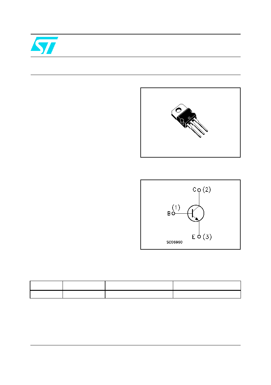
TO-220
Tube
BUL805
High voltage fast-switching NPN Power Transistor
General features
NPN Transistor
High voltage capability
Low spread of dynamic parameters
Minimum lot-to-lot spread for reliable operation
Very high switching speed
In compliance with the 2002/93/EC European
Directive
Description
The device is manufactured using high voltage
Multi-Epitaxial Planar technology for high
switching speeds and medium voltage capability.
It uses a Cellular Emitter structure with planar
edge termination to enhance switching speeds.
The device is designed for use as PFC in high
frequency ballast half Bridge voltage fed topology.
Applications
Electronic ballast for fluorescent lighting
Dedicated for PFC solution in half-bridge
voltage fed topology.
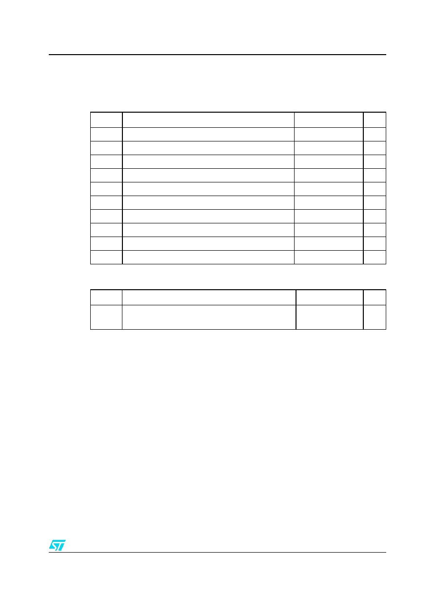
Internal schematic diagram
TO-220
1
2
3
www.st.com

BUL805
2/8
Contents
1
Electrical ratings . . . . . . . . . . . . . . . . . . . . . . . . . . . . . . . . . . . . . . . . . . . . 3
2
Electrical characteristics . . . . . . . . . . . . . . . . . . . . . . . . . . . . . . . . . . . . . 4
2.1
Electrical characteristics (curves) . . . . . . . . . . . . . . . . . . . . . . . . . . . . . . . . 5
2.2
Test circuits . . . . . . . . . . . . . . . . . . . . . . . . . . . . . . . . . . . . . . . . . . . . . . . . 6
3
Package mechanical data . . . . . . . . . . . . . . . . . . . . . . . . . . . . . . . . . . . . . 7
4
Revision history . . . . . . . . . . . . . . . . . . . . . . . . . . . . . . . . . . . . . . . . . . . . 9
BUL805
Electrical ratings
3/8
1
Electrical ratings
Table 2.
Thermal data
Table 1.
Absolute maximum rating
Symbol
Parameter
Value
Unit
V
CES
Collector-emitter voltage (V
BE
= 0)
800
V
V
CEO
Collector-emitter voltage (I
B
= 0)
450
V
V
EBO
Emitter-base voltage (I
C
= 0)
9
V
I
C
Collector current
5
A
I
CM
Collector peak current (t
P
< 5ms)
10
A
I
B
Base current
2
A
I
BM
Base peak current (t
P
< 5ms)
4
A
P
tot
Total dissipation at T
c
= 25°C
80
W
T
stg
Storage temperature
-65 to 150
°C
T
J
Max. operating junction temperature
150
°C
Symbol
Parameter
Value
Unit
R
thj-case
R
thj-amb
Thermal resistance junction-case
__
max
Thermal resistance junction-amb
__
max
1.56
62.5
°C/W
°C/W

Electrical characteristics
BUL805
4/8
2
Electrical
characteristics
(T
case
= 25°C unless otherwise specified)
Note (1) Pulsed duration = 300
µs, duty cycle 1.5%
Table 3.
Electrical characteristics
Symbol
Parameter
Test Conditions
Min.
Typ.
Max.
Unit
I
CES
Collector cut-off current
(V
BE
=-1.5V)
V
CE
=800V
V
CE
=800V
T
j
=125°C
100
500
µA
µA
I
CEO
Collector cut-off current
(I
B
=0)
V
CE
=450V
250
µA
V
EBO
Emitter-base voltage
(I
C
= 0)
I
E
=10mA
9
V
V
CEO(sus)
(1)
Collector-emitter
sustaining voltage
(I
B
= 0)
I
C
=100mA L =25mH
450
V
V
CE(sat)
(1)
Collector-emitter
saturation voltage
I
C
=1A I
B
=0.2A
I
C
=2A I
B
=0.4A
I
C
=3A I
B
=0.6A
0.4
0.6
0.8
V
V
V
V
BE(sat)
(1)
Base-emitter saturation
voltage
I
C
=1A I
B
=0.2A
I
C
=2A I
B
=0.4A
I
C
=3A I
B
=0.6A
1.1
1.3
1.5
V
V
V
h
FE
DC current gain
I
C
=10mA V
CE
=5V
I
C
=2A V
CE
=5V
10
10
20

BUL805
Package mechanical data
5/8
3 Package
mechanical
data
In order to meet environmental requirements, ST offers these devices in ECOPACK®
packages. These packages have a Lead-free second level interconnect. The category of
second level interconnect is marked on the package and on the inner box label, in
compliance with JEDEC Standard JESD97. The maximum ratings related to soldering
conditions are also marked on the inner box label. ECOPACK is an ST trademark.
ECOPACK specifications are available at:
www.st.com
Document Outline