 | –≠–ª–µ–∫—Ç—Ä–æ–Ω–Ω—ã–π –∫–æ–º–ø–æ–Ω–µ–Ω—Ç: BUZ80A | –°–∫–∞—á–∞—Ç—å:  PDF PDF  ZIP ZIP |

BUZ80A
N - CHANNEL 800V - 2.5
- 3.8A - TO-220
FAST POWER MOS TRANSISTOR
s
TYPICAL R
DS(on)
= 2.5
s
±
30V GATE TO SOURCE VOLTAGE RATING
s
100% AVALANCHE TESTED
s
REPETITIVE AVALANCHE DATA AT 100
o
C
s
LOW INTRINSIC CAPACITANCES
s
GATE CHARGE MINIMIZED
s
REDUCED THRESHOLD VOLTAGE SPREAD
APPLICATIONS
s
HIGH CURRENT, HIGH SPEED SWITCHING
s
SWITCH MODE POWER SUPPLIES (SMPS)
s
DC-AC CONVERTERS FOR WELDING
EQUIPMENT AND UNINTERRUPTIBLE
POWER SUPPLIES AND MOTOR DRIVE
Æ
INTERNAL SCHEMATIC DIAGRAM
ABSOLUTE MAXIMUM RATINGS
Symbol
Parameter
Value
Un it
BUZ80A
V
DS
Drain-source Voltage (V
GS
= 0)
800
V
V
DGR
Drain- gate Volt age (R
GS
= 20 k
)
800
V
V
GS
G ate-source Voltage
±
20
V
I
D
Drain Current (continuous) at T
c
= 25
o
C
3.8
A
I
D
Drain Current (continuous) at T
c
= 100
o
C
2.3
A
I
DM
(
∑
)
Drain Current (pulsed)
15
A
P
tot
T otal Dissipation at T
c
= 25
o
C
100
W
Derating Factor
0.8
W /
o
C
V
ISO
I nsulat ion W ithstand Voltage (DC)
V
T
s tg
Storage Temperat ure
-65 to 150
o
C
T
j
Max. Operating Junction Temperature
150
o
C
(
∑
) Pulse width limited by safe operating area
TYPE
V
DSS
R
DS(on)
I
D
BUZ80A
800 V
< 3
3. 8 A
November 1998
1
2
3
TO-220
1/9

THERMAL DATA
TO-220
R
thj -case
Thermal Resistance Junction-case
Max
1.25
o
C/W
R
thj -amb
R
thc-sink
T
l
Thermal Resistance Junction-ambient
Max
Thermal Resistance Case-sink
Typ
Maximum Lead Temperature For Soldering Purpose
62. 5
0. 5
300
o
C/W
o
C/W
o
C
AVALANCHE CHARACTERISTICS
Symbo l
Parameter
Max Valu e
Unit
I
AR
Avalanche Current , Repet itive or Not-Repet itive
(pulse width limited by T
j
max)
3. 8
A
E
AS
Single Pulse Avalanche Energy
(starting T
j
= 25
o
C, I
D
= I
AR
, V
DD
= 50 V)
200
mJ
ELECTRICAL CHARACTERISTICS (T
case
= 25
o
C unless otherwise specified)
OFF
Symbo l
Parameter
Test Con ditions
Min.
T yp.
Max.
Unit
V
(BR)DSS
Drain-source
Breakdown Voltage
I
D
= 250
µ
A
V
GS
= 0
800
V
I
DSS
Zero G ate Voltage
Drain Current (V
GS
= 0)
V
DS
= Max Rating
V
DS
= Max Rating x 0.8
T
c
= 100
o
C
250
1000
µ
A
µ
A
I
G SS
Gat e-body Leakage
Current (V
DS
= 0)
V
GS
=
±
20 V
±
100
nA
ON (
)
Symbo l
Parameter
Test Con ditions
Min.
T yp.
Max.
Unit
V
G S(th)
Gat e Threshold
Voltage
V
DS
= V
GS
I
D
= 250
µ
A
2
3
4
V
R
DS(on)
Static Drain-source O n
Resist ance
V
GS
= 10V
I
D
= 1.7 A
V
GS
= 10V
I
D
= 1.7 A
T
c
= 100
o
C
2.5
3
6
I
D(o n)
On Stat e Drain Current
V
DS
> I
D(o n)
x R
DS(on )ma x
V
GS
= 10 V
3. 8
A
DYNAMIC
Symbo l
Parameter
Test Con ditions
Min.
T yp.
Max.
Unit
g
f s
(
)
Forward
Transconduct ance
V
DS
> I
D(o n)
x R
DS(on )ma x
I
D
= 1.7A
1
S
C
iss
C
os s
C
rss
Input Capacitance
Out put Capacitance
Reverse T ransfer
Capacitance
V
DS
= 25 V
f = 1 MHz
V
GS
= 0
1100
150
35
pF
pF
pF
Æ
BUZ80A
2/9

ELECTRICAL CHARACTERISTICS (continued)
SWITCHING ON
Symbo l
Parameter
Test Con ditions
Min.
T yp.
Max.
Unit
t
d(on)
t
r
Turn-on Time
Rise Time
V
DD
= 30 V
I
D
= 2.3 A
R
G
= 50
V
GS
= 10 V
(see test circuit, figure 3)
65
150
90
200
ns
ns
(di/dt)
on
Turn-on Current Slope
V
DD
= 600 V
I
D
= 3.8 A
R
G
= 50
V
GS
= 10 V
(see test circuit, f igure 5)
80
110
A/
µ
s
Q
g
Q
gs
Q
gd
Tot al Gate Charge
Gat e-Source Charge
Gat e-Drain Charge
V
DD
= 400 V
I
D
= 5 A
V
GS
= 10 V
55
8
26
70
nC
nC
nC
SWITCHING OFF
Symbo l
Parameter
Test Con ditions
Min.
T yp.
Max.
Unit
t
r (Voff)
t
f
t
c
Off -volt age Rise Time
Fall Time
Cross-over Time
V
DD
= 600 V
I
D
= 3.8 A
R
G
= 50
V
GS
= 10 V
(see test circuit, figure 5)
110
140
150
145
190
200
ns
ns
ns
SOURCE DRAIN DIODE
Symbo l
Parameter
Test Con ditions
Min.
T yp.
Max.
Unit
I
SD
I
SDM
(
∑
)
Source-drain Current
Source-drain Current
(pulsed)
3. 8
15
A
A
V
SD
(
)
Forward On Volt age
I
SD
= 4 A
V
GS
= 0
2
V
t
rr
Q
rr
I
RRM
Reverse Recovery
Time
Reverse Recovery
Charge
Reverse Recovery
Current
I
SD
= 4 A
di/dt = 100 A/
µ
s
V
DD
= 100 V
T
j
= 150
o
C
(see test circuit, figure 5)
500
4.3
17
ns
µ
C
A
(
) Pulsed: Pulse duration = 300
µ
s, duty cycle 1.5 %
(
∑
) Pulse width limited by safe operating area
Safe Operating Area
Thermal Impedance
Æ
BUZ80A
3/9
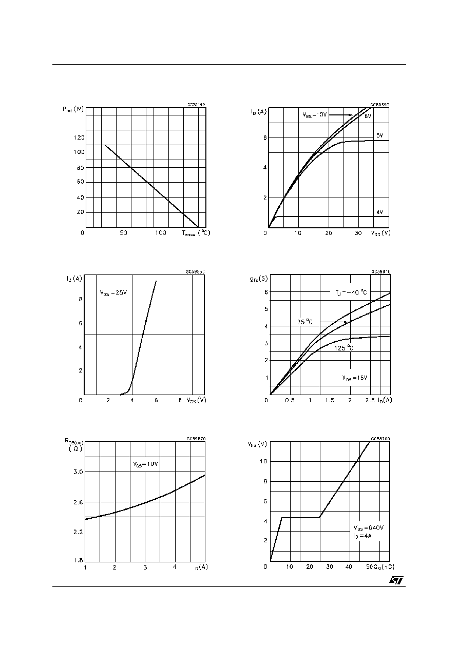
Derating Curve
Transfer Characteristics
Static Drain-source On Resistance
Output Characteristics
Transconductance
Gate Charge vs Gate-source Voltage
Æ
BUZ80A
4/9
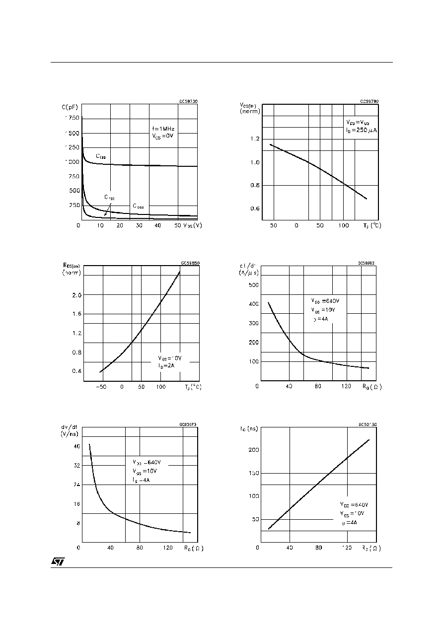
Capacitance Variations
Normalized On Resistance vs Temperature
Turn-off Drain-source Voltage Slope
Normalized Gate Threshold Voltage vs
Temperature
Turn-on Current Slope
Cross-over Time
Æ
BUZ80A
5/9

Switching Safe Operating Area
Source-drain Diode Forward Characteristics
Accidental Overload Area
Æ
BUZ80A
6/9
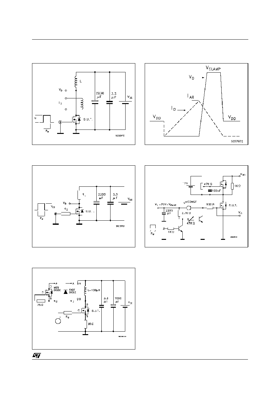
Fig. 1: Unclamped Inductive Load Test Circuit
Fig. 3: Switching Times Test Circuits For
Resistive Load
Fig. 2: Unclamped Inductive Waveform
Fig. 4: Gate Charge test Circuit
Fig. 5: Test Circuit For Inductive Load Switching
And Diode Recovery Times
Æ
BUZ80A
7/9

DIM.
mm
inch
MIN.
TYP.
MAX.
MIN.
TYP.
MAX.
A
4.40
4.60
0.173
0.181
C
1.23
1.32
0.048
0.051
D
2.40
2.72
0.094
0.107
D1
1.27
0.050
E
0.49
0.70
0.019
0.027
F
0.61
0.88
0.024
0.034
F1
1.14
1.70
0.044
0.067
F2
1.14
1.70
0.044
0.067
G
4.95
5.15
0.194
0.203
G1
2.4
2.7
0.094
0.106
H2
10.0
10.40
0.393
0.409
L2
16.4
0.645
L4
13.0
14.0
0.511
0.551
L5
2.65
2.95
0.104
0.116
L6
15.25
15.75
0.600
0.620
L7
6.2
6.6
0.244
0.260
L9
3.5
3.93
0.137
0.154
DIA.
3.75
3.85
0.147
0.151
L6
A
C
D
E
D1
F
G
L7
L2
Dia.
F1
L5
L4
H2
L9
F2
G1
TO-220 MECHANICAL DATA
P011C
Æ
BUZ80A
8/9

Information furnished is believed to be accurate and reliable. However, STMicroelectronics assumes no responsibility for the consequences
of use of such information nor for any infringement of patents or other rights of third parties which may result from its use. No license is
granted by implication or otherwise under any patent or patent rights of STMicroelectronics. Specification mentioned in this publication are
subject to change without notice. This publication supersedes and replaces all information previously supplied. STMicroelectronics products
are not authorized for use as critical components in life support devices or systems without express written approval of STMicroelectronics.
The ST logo is a registered trademark of STMicroelectronics
©
1998 STMicroelectronics ≠ Printed in Italy ≠ All Rights Reserved
STMicroelectronics GROUP OF COMPANIES
Australia - Brazil - Canada - China - France - Germany - Italy - Japan - Korea - Malaysia - Malta - Mexico - Morocco - The Netherlands -
Singapore - Spain - Sweden - Switzerland - Taiwan - Thailand - United Kingdom - U.S.A.
http://www.st.com
.
Æ
BUZ80A
9/9