 | –≠–ª–µ–∫—Ç—Ä–æ–Ω–Ω—ã–π –∫–æ–º–ø–æ–Ω–µ–Ω—Ç: BYW77 | –°–∫–∞—á–∞—Ç—å:  PDF PDF  ZIP ZIP |
BYW77G-200
Æ
October 1999 - Ed:3A
HIGH EFFICIENCY FAST RECOVERY DIODES
I
F(AV)
25 A
V
RRM
200 V
trr
50 ns
V
F
0.85 V
MAIN PRODUCT CHARACTERISTICS
VERY SMALL CONDUCTION LOSSES
NEGLIGIBLE SWITCHING LOSSES
LOW FORWARD AND REVERSE RECOVERY
TIME
HIGH SURGE CURRENT CAPABILITY
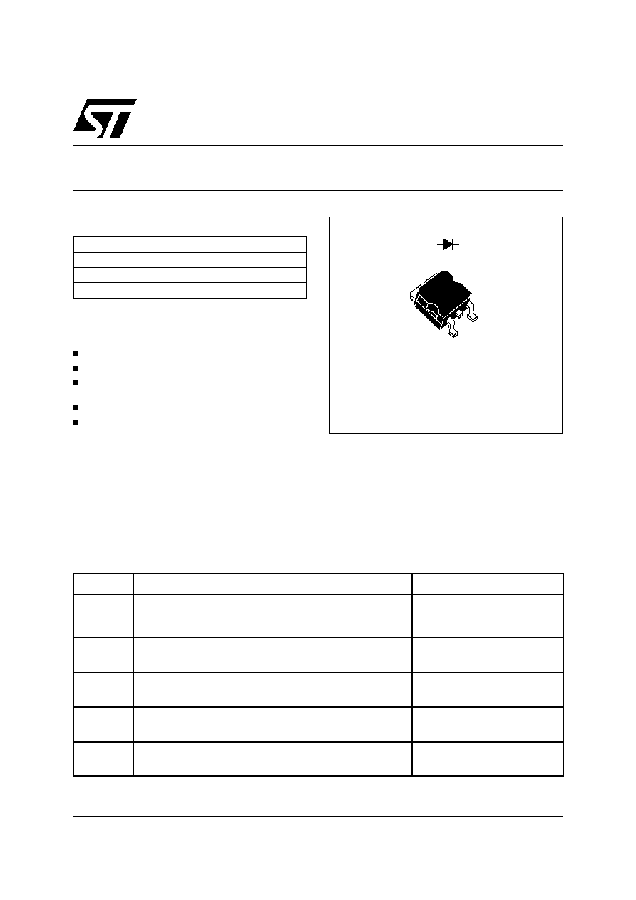
SMD PACKAGE
FEATURES AND BENEFITS
Single rectifier suited for switchmode power supply
and high frequency DC to DC converters.
Packaged in D
2
PAK, this surface mount device is
intended for use in high frequency inverters, free
wheeling and polarity protection applications.
DESCRIPTION
1
2
3
4
1 & 3
4
Symbol
Parameter
Value
Unit
V
RRM
Repetitive peak reverse voltage
200
V
I
F(RMS)
RMS forward current
50
A
I
F(AV)
Average forward current
Tc=125
∞
C
= 0.5
25
A
I
FSM
Surge non repetitive forward current
tp=10ms
sinusoidal
200
A
I
FRM
Repetitive peak forward current
tp = 5
µ
s
f = 5 kHz
310
A
Tstg
Tj
Storage and junction temperature range
- 40 to + 150
∞
C
ABSOLUTE MAXIMUM RATINGS
D
2
PAK
(Plastic)
1/5

Symbol
Parameter
Value
Unit
R
th (j-c)
Junction to case
1
∞
C/W
THERMAL RESISTANCE
Symbol
Parameter
Test Conditions
Min.
Typ.
Max.
Unit
I
R
*
Reverse leakage current
V
R
= V
RRM
T
j
= 25
∞
C
25
µ
A
T
j
= 100
∞
C
2.5
mA
V
F **
Forward voltage drop
I
F
= 20 A
T
j
= 125
∞
C
0.85
V
I
F
= 40 A
T
j
= 125
∞
C
1.00
I
F
= 40 A
T
j
= 25
∞
C
1.15
Pulse test :
* tp = 5 ms,
< 2 %
** tp = 380
µ
s,
< 2 %
To evaluate the conduction losses use the following equation :
P = 0.65 x I
F(AV)
+ 0.0075 I
F
2
(RMS)
STATIC ELECTRICAL CHARACTERISTICS
Symbol
Parameter
Test Conditions
Min.
Typ.
Max.
Unit
t
rr
Reverse recovery
time
T
j
= 25
∞
C
I
F
= 0.5A
Irr = 0.25 A
I
R
= 1A
35
ns
T
j
= 25
∞
C
I
F
= 1A
dI
F
/dt = -50A/
µ
s
V
R
=
30V
50
t
fr
Forward recovery
time
T
j
= 25
∞
C
I
F
= 1A
dI
F
/dt = 100A/
µ
s
V
FR
= 1.1 x V
F
max
10
ns
V
FP
Peak forward
voltage
T
j
= 25
∞
C
I
F
= 1A
dI
F
/dt = 100A/
µ
s
1.5
V
RECOVERY CHARACTERISTICS
PIN OUT configuration in D
2
PAK:
BYW77G-200
2/5

0
0.1 0.2 0.3 0.4 0.5 0.6 0.7 0.8 0.9
1
0
100
200
300
400
500
I M(A)
P=20W
P=30W
P=40W
T
I
M
=tp/T
tp
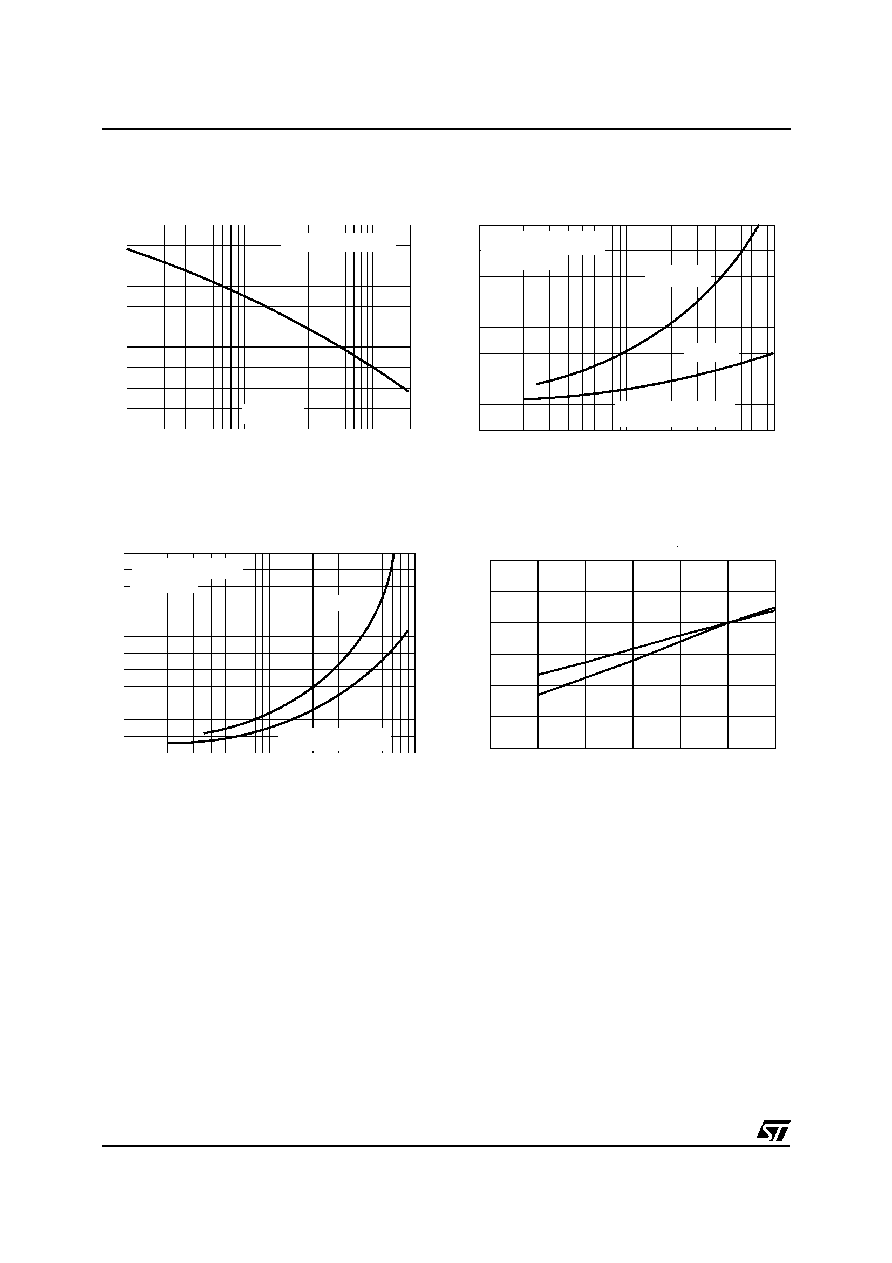
Fig.2 : Peak current versus form factor.
Tj= 125 C
o
IFM(A)
0.1
1
10
100
300
VFM(V)
0.0
0.2
0.4
0.6
0.8
1.0
1.2
1.4
1.6
1.8
Fig.3 : Forward voltage drop versus forward cur-
rent (maximum values).
0.1
1.0
0.2
0.5
Zth(j-c) (tp.
)
K =
Rth(j-c)
= 0 . 5
= 0 . 2
= 0 .1
Singl e puls e
tp(s)
T
=tp/T
tp
1.0E-03
1.0E-02
1.0E-01
1. 0E+00
K
Fig.4 : Relative variation of thermal impedance
junction to case versus pulse duration.
0
5
10
15
20
25
30
0.0
2.5
5.0
7.5
10.0
12.5
15.0
17.5
20.0
22.5
25.0
27.5
30.0
=0.05
=0.1
=0.2
=0.5
T
=tp/T
tp
IF(av)(A)
PF(av)(W)
=1
Fig.1 : Average forward power dissipation versus
average forward current.
0
20
40
60
80
100
120
140
160
0
5
10
15
20
25
30
T
=tp/T
tp
=0.5
F(av)(A)
I
o
Tamb( C)
Rth(j-a)=15
C/W
o
Rth(j-a)=Rth(j-c)
Fig.6 : Average current versus ambient tempera-
ture. (
= 0.5)
0.001
0.01
0.1
1
0
50
100
150
200
250
300
IM
t
=0.5
t(s)
IM(A)
Tc=25 C
o
Tc=75 C
o
Tc=125 C
o
Fig.5 : Non repetitive surge peak forward current
versus overload duration.
BYW77G-200
3/5
1
10
100
100
110
120
130
140
150
160
170
180
190
200
200
VR(V)
F=1MHz Tj=25 C
o
C(pF)
Fig.7 : Junction capacitance versus reverse volt-
age applied (Typical values).
1
10
1 00
0
10
20
30
40
50
60
70
80
QRR(nC)
90%CONFIDENCE
IF=IF(av)
Tj=100 C
O
Tj=25 C
O
dIF/dt(A/
µ
s)
Fig.8 : Reverse recovery charges versus dI
F
/dt.
Tj(
C)
QRR;IRM[Tj]/QRR;IRM[Tj=125 C]
0
25
50
75
100
125
150
0.00
0.25
0.50
0.75
1.00
1.25
1.50
IRM
QRR
o
o
Fig.10 : Dynamic parameters versus junction tem-
perature.
1
10
1 00
0.0
0.5
1.0
1.5
2.0
2.5
3.0
20
IRM(A)
dIF/dt(A/
µ
s)
90%CONFIDENCE
Tj=100 C
O
Tj=25 C
O
IF=IF(av)
Fig.9 : Peak reverse current versus dIF/dt.
BYW77G-200
4/5

PACKAGE MECHANICAL DATA
D
2
PAK (Plastic)
A
C2
D
R
2.0 MIN.
FLAT ZONE
A2
V2
C
A1
G
L
L3
L2
B
B2
E
Information furnished is believed to be accurate and reliable. However, STMicroelectronics assumes no responsibility for the consequences of
use of such information nor for any infringementof patents or other rights of third parties which may result from its use. No license is granted by
implication or otherwise under any patent or patent rights of STMicroelectronics. Specifications mentioned in this publication are subject to
change without notice. This publication supersedes and replaces all information previously supplied.
STMicroelectronics products are not authorized for use as critical components in life support devices or systems without express written ap-
proval of STMicroelectronics.
The ST logo is a registered trademark of STMicroelectronics
©
1999 STMicroelectronics - Printed in Italy - All rights reserved.
STMicroelectronics GROUP OF COMPANIES
Australia - Brazil - China - Finland - France - Germany - Hong Kong - India - Italy - Japan - Malaysia
Malta - Morocco - Singapore - Spain - Sweden - Switzerland - United Kingdom - U.S.A.
http://www.st.com
REF.
DIMENSIONS
Millimeters
Inches
Min.
Max.
Min.
Max.
A
4.40
4.60
0.173
0.181
A1
2.49
2.69
0.098
0.106
A2
0.03
0.23
0.001
0.009
B
0.70
0.93
0.027
0.037
B2
1.14
1.70
0.045
0.067
C
0.45
0.60
0.017
0.024
C2
1.23
1.36
0.048
0.054
D
8.95
9.35
0.352
0.368
E
10.00
10.40
0.393
0.409
G
4.88
5.28
0.192
0.208
L
15.00
15.85
0.590
0.624
L2
1.27
1.40
0.050
0.055
L3
1.40
1.75
0.055
0.069
M
2.40
3.20
0.094
0.126
R
0.40 typ.
0.016 typ.
V2
0
∞
8
∞
0
∞
8
∞
FOOT PRINT (in millimeters)
8.90
3.70
1.30
5.08
16.90
10.30
BYW77G-200
5/5