Document Outline
- FEATURES SUMMARY
- SUMMARY DESCRIPTION
- PIN DESCRIPTION
- ARCHITECTURAL OVERVIEW
- RUNTIME CONTROL REGISTER DEFINITION
- DETAILED OPERATION
- INSTRUCTIONS
- PROGRAMMING FLASH MEMORY
- PLDs
- DSP BUS INTERFACE
- I/O PORTS
- POWER MANAGEMENT
- RESET TIMING AND DEVICE STATUS AT RESET
- PROGRAMMING IN-CIRCUIT USING JTAG ISP
- INITIAL DELIVERY STATE
- AC AND DC PARAMETERS
- MAXIMUM RATING
- DC AND AC OPERATING AND MEASUREMENT CONDITIONS
- PACKAGE MECHANICAL
- PART NUMBERING
- APPENDIX A. TQFP80 PIN ASSIGNMENTS
- APPENDIX B. CSIOP REGISTER BIT DEFINITIONS
- Table 34. Data-In Registers Ö Ports A, B, C, D, E, G
- Table 35. Data-Out Registers Ö Ports A, B, C, D, E, G
- Table 36. Direction Registers Ö Ports A, B, C, D, E, G
- Table 37. Drive Registers Ö Ports A, B, E, G
- Table 38. Drive Registers Ö Port C
- Table 39. Enable-Out Registers Ö Ports A, B, C
- Table 40. Input Macrocells Ö Ports A, B, C
- Table 41. Output Macrocells A Register
- Table 42. Output Macrocells B Register
- Table 43. Mask Macrocells A Register
- Table 44. Mask Macrocells B Register
- Table 45. Flash Memory Protection Register
- Table 46. Flash Boot Protection Register
- Table 47. JTAG Enable Register
- Table 48. Page Register
- Table 49. PMMR0 Register
- Table 50. PMMR2 Register
- Table 51. Memory_ID0 Register
- Table 52. Memory_ID1 Register
- REVISION HISTORY
1/73
August 2004
DSM2150F5V
DSM (Digital Signal Processor System Memory)
for Analog Devices DSPs (3.3V Supply)
FEATURES SUMMARY
s
Glueless Connection to DSP
≠
Easily add memory, logic, and I/O to the
External Port of ADSP-218x, 219x, 2106x,
2116x, 2153x, and TS101 families of
DSPs from Analog Devices, Inc.
s
Dual Flash Memories
≠
Two independent Flash memory arrays
for storing DSP code and data
≠
Capable of read-while-write concurrent
Flash memory operation
≠
Device can be configured as 8-bit or 16-bit
≠
Built-in programmable address decoding
logic allows mapping individual sectors of
each Flash array to any address boundary
≠
Each Flash sector can be write protected
s
512 KByte Main Flash memory
≠
Ample storage for boot loading DSP code/
data upon reset and subsequent code
swaps
≠
Large capacity for storing tables and
constants or for data recording
s
32 KByte Secondary Flash memory
≠
Smaller sector size ideal for storing
calibration and configuration constants.
Eliminate external serial EEPROM.
≠
Optionally bypass internal DSP boot ROM
during start-up and execute code directly
from Secondary Flash. Use for custom
start-up code and In-Application
Programming (IAP).
s
Up to 40 Multifunction I/O Pins
≠
Increase total DSP system I/O capability
≠
I/O controlled by DSP software or PLD
logic
s
General purpose PLD
≠
Use for peripheral glue logic to keypads,
control panel, displays, LCDs, and other
devices
≠
Over 3,000 gates of PLD with 16 macro
cells
≠
Eliminate PLDs and external logic devices
≠
Create state machines, chip selects,
simple shifters and counters, clock
dividers, delays
≠
Simple PSDsoft Express
TM
development
software, free from www.st.com/psm
Figure 1. TQFP 80-pin Package
s
In-System Programming (ISP) with JTAG
≠
Program entire chip in 15-35 seconds with
no involvement of the DSP
≠
Optionally links with DSP JTAG debug
port
≠
Eliminate need for sockets and pre-
programming of memory and logic
devices
≠
ISP allows efficient manufacturing and
product testing supporting Just-In-Time
inventory
≠
Use low-cost FlashLINK
TM
cable with any
PC. Available from www.st.com/psm.
s
Content Security
≠
Programmable Security Bit blocks access
of device programmers and readers
s
Operating Range
≠
V
CC
: 3.3V ± 10%, Temp: ≠40∞C to +85∞C
s
Zero-Power Technology
≠
50µA standby current typical
s
Flash Memory Speed, Endurance, Retention
≠
120ns, 100K cycles, 15 year retention
TQFP80 (T)

DSM2150F5V
2/73
TABLE OF CONTENTS
FEATURES SUMMARY . . . . . . . . . . . . . . . . . . . . . . . . . . . . . . . . . . . . . . . . . . . . . . . . . . . . . . . . . . . . . 1
SUMMARY DESCRIPTION . . . . . . . . . . . . . . . . . . . . . . . . . . . . . . . . . . . . . . . . . . . . . . . . . . . . . . . . . . . 5
PIN DESCRIPTION . . . . . . . . . . . . . . . . . . . . . . . . . . . . . . . . . . . . . . . . . . . . . . . . . . . . . . . . . . . . . . . . . 8
ARCHITECTURAL OVERVIEW . . . . . . . . . . . . . . . . . . . . . . . . . . . . . . . . . . . . . . . . . . . . . . . . . . . . . . 10
DSP Address/Data/Control Interface . . . . . . . . . . . . . . . . . . . . . . . . . . . . . . . . . . . . . . . . . . . . . . 10
Main Flash Memory . . . . . . . . . . . . . . . . . . . . . . . . . . . . . . . . . . . . . . . . . . . . . . . . . . . . . . . . . . . . 11
Secondary Flash Memory . . . . . . . . . . . . . . . . . . . . . . . . . . . . . . . . . . . . . . . . . . . . . . . . . . . . . . . 11
Programmable Logic (PLDs) . . . . . . . . . . . . . . . . . . . . . . . . . . . . . . . . . . . . . . . . . . . . . . . . . . . . 11
Runtime Control Registers . . . . . . . . . . . . . . . . . . . . . . . . . . . . . . . . . . . . . . . . . . . . . . . . . . . . . . 12
Memory Page Register . . . . . . . . . . . . . . . . . . . . . . . . . . . . . . . . . . . . . . . . . . . . . . . . . . . . . . . . . 12
I/O Ports . . . . . . . . . . . . . . . . . . . . . . . . . . . . . . . . . . . . . . . . . . . . . . . . . . . . . . . . . . . . . . . . . . . . . 12
JTAG ISP Port . . . . . . . . . . . . . . . . . . . . . . . . . . . . . . . . . . . . . . . . . . . . . . . . . . . . . . . . . . . . . . . . 12
Power Management. . . . . . . . . . . . . . . . . . . . . . . . . . . . . . . . . . . . . . . . . . . . . . . . . . . . . . . . . . . . 12
Security and NVM Sector Protection . . . . . . . . . . . . . . . . . . . . . . . . . . . . . . . . . . . . . . . . . . . . . . 12
RUNTIME CONTROL REGISTER DEFINITION . . . . . . . . . . . . . . . . . . . . . . . . . . . . . . . . . . . . . . . . . . 13
DETAILED OPERATION. . . . . . . . . . . . . . . . . . . . . . . . . . . . . . . . . . . . . . . . . . . . . . . . . . . . . . . . . . . . 14
Flash Memories . . . . . . . . . . . . . . . . . . . . . . . . . . . . . . . . . . . . . . . . . . . . . . . . . . . . . . . . . . . . . . . 14
INSTRUCTIONS . . . . . . . . . . . . . . . . . . . . . . . . . . . . . . . . . . . . . . . . . . . . . . . . . . . . . . . . . . . . . . . . . . 19
Reading Flash Memory . . . . . . . . . . . . . . . . . . . . . . . . . . . . . . . . . . . . . . . . . . . . . . . . . . . . . . . . . 20
Read Memory Contents . . . . . . . . . . . . . . . . . . . . . . . . . . . . . . . . . . . . . . . . . . . . . . . . . . . . . . . . 20
Read Main Flash Identifier . . . . . . . . . . . . . . . . . . . . . . . . . . . . . . . . . . . . . . . . . . . . . . . . . . . . . . 20
Read Memory Sector Protection Status . . . . . . . . . . . . . . . . . . . . . . . . . . . . . . . . . . . . . . . . . . . 20
Reading the Erase/Program Status Bits . . . . . . . . . . . . . . . . . . . . . . . . . . . . . . . . . . . . . . . . . . . 20
Data Polling Flag (DQ7). . . . . . . . . . . . . . . . . . . . . . . . . . . . . . . . . . . . . . . . . . . . . . . . . . . . . . . . . 20
Toggle Flag (DQ6) . . . . . . . . . . . . . . . . . . . . . . . . . . . . . . . . . . . . . . . . . . . . . . . . . . . . . . . . . . . . . 21
Error Flag (DQ5). . . . . . . . . . . . . . . . . . . . . . . . . . . . . . . . . . . . . . . . . . . . . . . . . . . . . . . . . . . . . . . 21
Erase Time-out Flag (DQ3) . . . . . . . . . . . . . . . . . . . . . . . . . . . . . . . . . . . . . . . . . . . . . . . . . . . . . . 21
PROGRAMMING FLASH MEMORY. . . . . . . . . . . . . . . . . . . . . . . . . . . . . . . . . . . . . . . . . . . . . . . . . . . 22
PLDs . . . . . . . . . . . . . . . . . . . . . . . . . . . . . . . . . . . . . . . . . . . . . . . . . . . . . . . . . . . . . . . . . . . . . . . . . . . 24
Turbo Bit. . . . . . . . . . . . . . . . . . . . . . . . . . . . . . . . . . . . . . . . . . . . . . . . . . . . . . . . . . . . . . . . . . . . . 24
Decode PLD (DPLD) . . . . . . . . . . . . . . . . . . . . . . . . . . . . . . . . . . . . . . . . . . . . . . . . . . . . . . . . . . . 26
Complex PLD (CPLD) . . . . . . . . . . . . . . . . . . . . . . . . . . . . . . . . . . . . . . . . . . . . . . . . . . . . . . . . . . 27
Output Macrocell (OMC) . . . . . . . . . . . . . . . . . . . . . . . . . . . . . . . . . . . . . . . . . . . . . . . . . . . . . . . . 28
Product Term Allocator. . . . . . . . . . . . . . . . . . . . . . . . . . . . . . . . . . . . . . . . . . . . . . . . . . . . . . . . . 29
Loading and Reading the OMCs . . . . . . . . . . . . . . . . . . . . . . . . . . . . . . . . . . . . . . . . . . . . . . . . . 29
The OMC Mask Register . . . . . . . . . . . . . . . . . . . . . . . . . . . . . . . . . . . . . . . . . . . . . . . . . . . . . . . . 31

3/73
DSM2150F5V
The Output Enable of the OMC . . . . . . . . . . . . . . . . . . . . . . . . . . . . . . . . . . . . . . . . . . . . . . . . . . 31
Input Macrocells (IMC) . . . . . . . . . . . . . . . . . . . . . . . . . . . . . . . . . . . . . . . . . . . . . . . . . . . . . . . . . 31
DSP BUS INTERFACE . . . . . . . . . . . . . . . . . . . . . . . . . . . . . . . . . . . . . . . . . . . . . . . . . . . . . . . . . . . . . 33
Typical Memory Map, DSM2150F5V and ADSP21535 BLACKFIN DSP. . . . . . . . . . . . . . . . . . . 33
Specifying the Memory Map with PSDsoft ExpressTM . . . . . . . . . . . . . . . . . . . . . . . . . . . . . . . . 33
ADSP-21535 Blackfin DSP . . . . . . . . . . . . . . . . . . . . . . . . . . . . . . . . . . . . . . . . . . . . . . . . . . . . . . 36
ADSP-21062 SHARC DSP . . . . . . . . . . . . . . . . . . . . . . . . . . . . . . . . . . . . . . . . . . . . . . . . . . . . . . . 37
ADSP-TS101S TigerSHARC DSP . . . . . . . . . . . . . . . . . . . . . . . . . . . . . . . . . . . . . . . . . . . . . . . . . 38
ADSP-2191 . . . . . . . . . . . . . . . . . . . . . . . . . . . . . . . . . . . . . . . . . . . . . . . . . . . . . . . . . . . . . . . . . . . 39
ADSP-2188M . . . . . . . . . . . . . . . . . . . . . . . . . . . . . . . . . . . . . . . . . . . . . . . . . . . . . . . . . . . . . . . . . 40
I/O PORTS . . . . . . . . . . . . . . . . . . . . . . . . . . . . . . . . . . . . . . . . . . . . . . . . . . . . . . . . . . . . . . . . . . . . . . . 41
General Port Architecture . . . . . . . . . . . . . . . . . . . . . . . . . . . . . . . . . . . . . . . . . . . . . . . . . . . . . . . 41
Port Operating Modes . . . . . . . . . . . . . . . . . . . . . . . . . . . . . . . . . . . . . . . . . . . . . . . . . . . . . . . . . . 41
MCU I/O Mode . . . . . . . . . . . . . . . . . . . . . . . . . . . . . . . . . . . . . . . . . . . . . . . . . . . . . . . . . . . . . . . . 42
Drive Select Register. . . . . . . . . . . . . . . . . . . . . . . . . . . . . . . . . . . . . . . . . . . . . . . . . . . . . . . . . . . 43
DSP Data Bus. . . . . . . . . . . . . . . . . . . . . . . . . . . . . . . . . . . . . . . . . . . . . . . . . . . . . . . . . . . . . . . . . 43
PLD Inputs . . . . . . . . . . . . . . . . . . . . . . . . . . . . . . . . . . . . . . . . . . . . . . . . . . . . . . . . . . . . . . . . . . . 43
PLD Outputs. . . . . . . . . . . . . . . . . . . . . . . . . . . . . . . . . . . . . . . . . . . . . . . . . . . . . . . . . . . . . . . . . . 43
JTAG In-System Programming (ISP) . . . . . . . . . . . . . . . . . . . . . . . . . . . . . . . . . . . . . . . . . . . . . . 43
Enable Out . . . . . . . . . . . . . . . . . . . . . . . . . . . . . . . . . . . . . . . . . . . . . . . . . . . . . . . . . . . . . . . . . . . 43
Ports A, B, and C ≠ Functionality and Structure . . . . . . . . . . . . . . . . . . . . . . . . . . . . . . . . . . . . 44
Port D ≠ Functionality and Structure . . . . . . . . . . . . . . . . . . . . . . . . . . . . . . . . . . . . . . . . . . . . . . 45
Port E ≠ Functionality and Structure . . . . . . . . . . . . . . . . . . . . . . . . . . . . . . . . . . . . . . . . . . . . . . 46
Port F ≠ Functionality and Structure . . . . . . . . . . . . . . . . . . . . . . . . . . . . . . . . . . . . . . . . . . . . . . 46
Port G ≠ Functionality and Structure . . . . . . . . . . . . . . . . . . . . . . . . . . . . . . . . . . . . . . . . . . . . . . 46
POWER MANAGEMENT . . . . . . . . . . . . . . . . . . . . . . . . . . . . . . . . . . . . . . . . . . . . . . . . . . . . . . . . . . . 47
RESET TIMING AND DEVICE STATUS AT RESET . . . . . . . . . . . . . . . . . . . . . . . . . . . . . . . . . . . . . . 48
Power On Reset . . . . . . . . . . . . . . . . . . . . . . . . . . . . . . . . . . . . . . . . . . . . . . . . . . . . . . . . . . . . . . . 48
Warm Reset . . . . . . . . . . . . . . . . . . . . . . . . . . . . . . . . . . . . . . . . . . . . . . . . . . . . . . . . . . . . . . . . . . 48
I/O Pin, Register, and PLD Status at Reset . . . . . . . . . . . . . . . . . . . . . . . . . . . . . . . . . . . . . . . . . 48
PROGRAMMING IN-CIRCUIT USING JTAG ISP. . . . . . . . . . . . . . . . . . . . . . . . . . . . . . . . . . . . . . . . . 49
Standard JTAG Signals. . . . . . . . . . . . . . . . . . . . . . . . . . . . . . . . . . . . . . . . . . . . . . . . . . . . . . . . . 49
JTAG Extensions . . . . . . . . . . . . . . . . . . . . . . . . . . . . . . . . . . . . . . . . . . . . . . . . . . . . . . . . . . . . . . 50
INITIAL DELIVERY STATE. . . . . . . . . . . . . . . . . . . . . . . . . . . . . . . . . . . . . . . . . . . . . . . . . . . . . . . . . . 50
AC AND DC PARAMETERS. . . . . . . . . . . . . . . . . . . . . . . . . . . . . . . . . . . . . . . . . . . . . . . . . . . . . . . . . 51
MAXIMUM RATING. . . . . . . . . . . . . . . . . . . . . . . . . . . . . . . . . . . . . . . . . . . . . . . . . . . . . . . . . . . . . . . . 52
DC AND AC OPERATING AND MEASUREMENT CONDITIONS . . . . . . . . . . . . . . . . . . . . . . . . . . . . 53

DSM2150F5V
4/73
PACKAGE MECHANICAL . . . . . . . . . . . . . . . . . . . . . . . . . . . . . . . . . . . . . . . . . . . . . . . . . . . . . . . . . . 65
PART NUMBERING . . . . . . . . . . . . . . . . . . . . . . . . . . . . . . . . . . . . . . . . . . . . . . . . . . . . . . . . . . . . . . . 67
APPENDIX A.TQFP80 PIN ASSIGNMENTS . . . . . . . . . . . . . . . . . . . . . . . . . . . . . . . . . . . . . . . . . . . . 68
APPENDIX B.CSIOP REGISTER BIT DEFINITIONS . . . . . . . . . . . . . . . . . . . . . . . . . . . . . . . . . . . . . . 69
REVISION HISTORY. . . . . . . . . . . . . . . . . . . . . . . . . . . . . . . . . . . . . . . . . . . . . . . . . . . . . . . . . . . . . . . 72
5/73
DSM2150F5V
SUMMARY DESCRIPTION
The DSM2150F5V is an 8 or 16-bit system mem-
ory device for use with the Analog Devices DSPs.
DSM means Digital signal processor System
Memory. A DSM device brings In-System Pro-
grammable (ISP) Flash memory, parameter stor-
age, programmable logic, and additional I/O to
DSP systems. The result is a flexible two-chip so-
lution for DSP designs. On-chip integrated memo-
ry decode logic makes it easy to map dual banks
of Flash memory to the DSPs in a variety of ways
for bootloading or bypassing DSP boot ROM, code
execution, data recording, code swapping, and
parameter storage.
JTAG ISP reduces development time, simplifies
manufacturing flow, and lowers the cost of field up-
grades. The JTAG ISP interface eliminates the
need for sockets and pre-programmed memory
and logic devices. End products may be manufac-
tured with a blank DSM device soldered down and
programmed at the end of the assembly line in 15
to 35 seconds with no involvement of the DSP.
Rapidly program test code, then application code
as determined by Just-In Time inventory require-
ments. Additionally, JTAG ISP reduces develop-
ment time by turning fast iterations of DSP code in
the lab. Code updates in the field require no prod-
uct disassembly. The FlashLINK
TM
JTAG program-
ming cable costs $59 USD and plugs into any PC
parallel port. Programming through conventional
device insertion programmers is also available us-
ing PSDpro from STMicroelectronics and other 3rd
party programmers. See www.st.com/psm.
DSM devices add programmable logic (PLD) and
up to 32 configurable I/O pins to the DSP system.
The state of I/O pins can be driven by DSP soft-
ware or PLD logic. PLD and I/O configuration are
programmable by JTAG ISP. The PLD consists of
more than 3000 gates and has 16 macro cell reg-
isters. Common uses for the PLD include chip-se-
lects for external devices, state-machines, simple
shiftier and counters, keypad and control panel in-
terfaces, clock dividers, handshake delay, muxes,
etc., eliminating the need for small external PLDs
and logic devices. Configuration of PLD, I/O, and
Flash memory mapping is easily entered in a
point-and-click environment using the software
development tool, PSDsoft Express
TM
, available at
no charge from www.st.com/psm. The two-chip
DSP/DSM combination is ideal for systems having
limitations on size, EMI levels, and power con-
sumption. DSM memory and logic are "zero-pow-
er", meaning they automatically go to standby
between memory accesses or logic input chang-
es, producing low active and standby current con-
sumption, which is ideal for battery powered
products.
A programmable security bit in the DSM protects
its contents from unauthorized viewing and copy-
ing. When set, the security bit will block access of
programming devices (JTAG or others) to the
DSM Flash memories and PLD configuration. The
only way to defeat the security bit is to erase the
entire DSM device, after which the device is blank
and may be used again. The DSP will always have
access to Flash memory contents through the data
bus, even with security bit set.
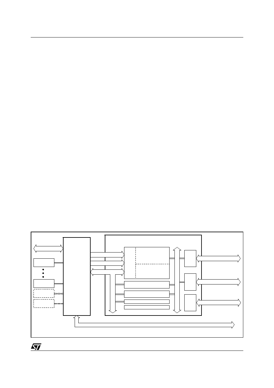
Figure 2. System Block Diagram, Two Chip Solution
AI05732
ADD
R
&
D
E
CO
D
E
LOGIC
PRIMARY
FLASH MEMORY
512 Kbytes
16 MACROCELL PLD
I/O CONTROL
POWER MANAGEMENT
CONTENT SECURITY
JTAG
ISP TO
ALL
AREAS
8 to 16
I/O
PORTS
16 I/O
PORTS
WITH
PLD
ADDRESS
8 or 16 DATA
CONTROL
DSM2150F5V
DSP SYSTEM MEMORY
ANALOG
DEVICES
DSP
ADSP-218x
ADSP-219x
ADSP-2153x
ADSP-2106x
ADSP-2116x
ADSP-TS101S
JTAG ISP
JTAG DEBUG (All But ADSP-218x Family)
SECONDARY
FLASH MEMORY
32 Kbytes
I/O FLAGS
SDRAM
HOST
MCU
SERIAL
DEVICE
SERIAL
DEVICE
I/O, PLD, CHIP SELECTS
GENERAL PURPOSE I/O
I/
O
B
U
S