1/63
December 2001
DSM2180F3
DSM (Digital Signal Processor System Memory)
For Analog Devices ADSP-218X Family (5V Supply)
FEATURES SUMMARY
s
Glueless Connection to DSP
≠ Easily add memory, logic, and I/O to DSP
s
128K Byte Flash Memory
≠ For Bootloading and/or Data Overlay Memory
≠ Programmable Decoding and Paging Logic
allows accessing Flash memory as Byte DMA
(BDMA) and as External Data Overlay mem-
ory
≠ Rapidly access Flash memory with BDMA for
booting and loading internal DSP Overlay
memory. Alternatively access the same Flash
memory as External Data Overlay memory to
efficiently write Flash memory with code up-
dates and data, a byte at a time with no DMA
setup overhead
≠ Individual 16K Byte Flash memory sectors
match size of DSP External Data Overlay
window for efficient data management. Inte-
grated page logic provides easy DSP access
to all 128K Bytes.
≠ DSM connects to lower byte of 16-bit DSP
data bus. Byte-wide accesses to 8-bit BDMA
space. Half-word accesses to 16-bit Data
Memory Overlay and 16-bit I/O Mem space.
s
5V Devices (±10%)
s
Up to 16 Multifunction I/O Pins
≠ Increase total DSP system I/O capability
≠ I/O controlled by DSP software or PLD logic
≠ 8mA I/O pin drive at 5 Vcc
s
General purpose PLD
≠ Over 3,000 Gates of PLD with 16 macro cells
≠ Use for peripheral glue logic to keypads, con-
trol panel, displays, LCD, UART devices, etc.
≠ Eliminate PLDs and external logic devices
≠ Create state machines, chip selects, simple
shifters and counters, clock dividers, delays
≠ Simple PSDsoft Express
TM
software ...Free
Figure 1. Packages
s
In-System Programming (ISP) with JTAG
≠ Program entire chip in 10-20 seconds with no
involvement of the DSP
≠ Eliminate sockets for pre-programmed mem-
ory and logic devices
≠ Efficient manufacturing allows easy product
testing and Just-In-Time inventory
≠ Use low-cost FlashLINK
TM
cable with PC
s
Content Security
≠ Programmable Security Bit blocks access of
device programmers and readers
s
Zero-Power Technology
≠ 75
µ
A standby at V
CC
=5V
s
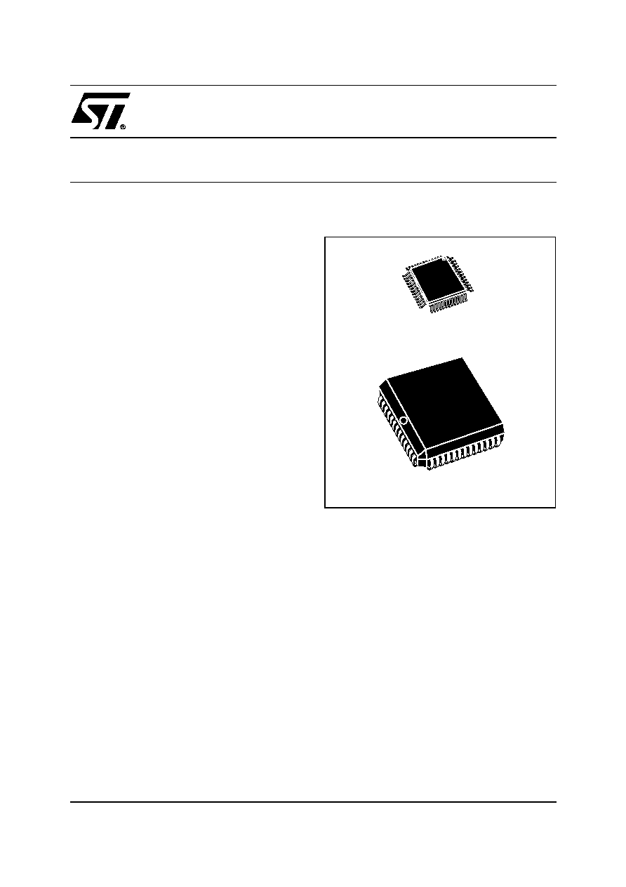
Small Packaging
≠ 52-pin PQFP or 52-pin PLCC
s
Memory Speed
≠ 90 ns
PLCC52 (K)
PQFP52 (T)

DSM2180F3
2/63
TABLE OF CONTENTS
Summary Description . . . . . . . . . . . . . . . . . . . . . . . . . . . . . . . . . . . . . . . . . . . . . . . . . . . . . . . . . . . . . . 4
Architectural Overview . . . . . . . . . . . . . . . . . . . . . . . . . . . . . . . . . . . . . . . . . . . . . . . . . . . . . . . . . . . . . 7
DSP Address/Data/Control Interface . . . . . . . . . . . . . . . . . . . . . . . . . . . . . . . . . . . . . . . . . . . . . . . . . 7
Flash Memory . . . . . . . . . . . . . . . . . . . . . . . . . . . . . . . . . . . . . . . . . . . . . . . . . . . . . . . . . . . . . . . . . . 7
Programmable Logic (PLDs) . . . . . . . . . . . . . . . . . . . . . . . . . . . . . . . . . . . . . . . . . . . . . . . . . . . . . . . 8
Runtime Control Registers . . . . . . . . . . . . . . . . . . . . . . . . . . . . . . . . . . . . . . . . . . . . . . . . . . . . . . . . 9
Memory Page Register . . . . . . . . . . . . . . . . . . . . . . . . . . . . . . . . . . . . . . . . . . . . . . . . . . . . . . . . . . . 9
I/O Ports . . . . . . . . . . . . . . . . . . . . . . . . . . . . . . . . . . . . . . . . . . . . . . . . . . . . . . . . . . . . . . . . . . . . . . 9
JTAG ISP Port . . . . . . . . . . . . . . . . . . . . . . . . . . . . . . . . . . . . . . . . . . . . . . . . . . . . . . . . . . . . . . . . . . 9
Power Management . . . . . . . . . . . . . . . . . . . . . . . . . . . . . . . . . . . . . . . . . . . . . . . . . . . . . . . . . . . . . 9
Security and NVM Sector Protection . . . . . . . . . . . . . . . . . . . . . . . . . . . . . . . . . . . . . . . . . . . . . . . . . 9
Pin Assignments . . . . . . . . . . . . . . . . . . . . . . . . . . . . . . . . . . . . . . . . . . . . . . . . . . . . . . . . . . . . . . . . 9
Typical connections . . . . . . . . . . . . . . . . . . . . . . . . . . . . . . . . . . . . . . . . . . . . . . . . . . . . . . . . . . . . . . 11
Memory Map . . . . . . . . . . . . . . . . . . . . . . . . . . . . . . . . . . . . . . . . . . . . . . . . . . . . . . . . . . . . . . . . . . . . . 13
Specifying Mem Map with PSDsoft ExpressTM . . . . . . . . . . . . . . . . . . . . . . . . . . . . . . . . . . . . . . . . 15
Runtime control register definition . . . . . . . . . . . . . . . . . . . . . . . . . . . . . . . . . . . . . . . . . . . . . . . . . . 17
Detailed Operation . . . . . . . . . . . . . . . . . . . . . . . . . . . . . . . . . . . . . . . . . . . . . . . . . . . . . . . . . . . . . . . . 18
Flash Memory . . . . . . . . . . . . . . . . . . . . . . . . . . . . . . . . . . . . . . . . . . . . . . . . . . . . . . . . . . . . . . . . . 18
Instruction Sequences . . . . . . . . . . . . . . . . . . . . . . . . . . . . . . . . . . . . . . . . . . . . . . . . . . . . . . . . . . . 20
Reading Flash Memory . . . . . . . . . . . . . . . . . . . . . . . . . . . . . . . . . . . . . . . . . . . . . . . . . . . . . . . . . . 20
Programming Flash Memory . . . . . . . . . . . . . . . . . . . . . . . . . . . . . . . . . . . . . . . . . . . . . . . . . . . . . . 21
Erasing Flash Memory. . . . . . . . . . . . . . . . . . . . . . . . . . . . . . . . . . . . . . . . . . . . . . . . . . . . . . . . . . . 23
Flash Memory Sector Protect. . . . . . . . . . . . . . . . . . . . . . . . . . . . . . . . . . . . . . . . . . . . . . . . . . . . . . 24
DSM Security Bit . . . . . . . . . . . . . . . . . . . . . . . . . . . . . . . . . . . . . . . . . . . . . . . . . . . . . . . . . . . . . . . 25
Reset Flash . . . . . . . . . . . . . . . . . . . . . . . . . . . . . . . . . . . . . . . . . . . . . . . . . . . . . . . . . . . . . . . . . . . 25
Page Register . . . . . . . . . . . . . . . . . . . . . . . . . . . . . . . . . . . . . . . . . . . . . . . . . . . . . . . . . . . . . . . . . 25
PLDs . . . . . . . . . . . . . . . . . . . . . . . . . . . . . . . . . . . . . . . . . . . . . . . . . . . . . . . . . . . . . . . . . . . . . . . . 25
Decode PLD (DPLD). . . . . . . . . . . . . . . . . . . . . . . . . . . . . . . . . . . . . . . . . . . . . . . . . . . . . . . . . . . . . . . 27
Complex PLD (CPLD) . . . . . . . . . . . . . . . . . . . . . . . . . . . . . . . . . . . . . . . . . . . . . . . . . . . . . . . . . . . . . 28

3/63
DSM2180F3
DSP Bus Interface . . . . . . . . . . . . . . . . . . . . . . . . . . . . . . . . . . . . . . . . . . . . . . . . . . . . . . . . . . . . . . 32
I/O Ports . . . . . . . . . . . . . . . . . . . . . . . . . . . . . . . . . . . . . . . . . . . . . . . . . . . . . . . . . . . . . . . . . . . . . 32
Port Operating Modes . . . . . . . . . . . . . . . . . . . . . . . . . . . . . . . . . . . . . . . . . . . . . . . . . . . . . . . . . . . 33
Port B ≠ Functionality and Structure . . . . . . . . . . . . . . . . . . . . . . . . . . . . . . . . . . . . . . . . . . . . . . . . 35
Port C ≠ Functionality and Structure . . . . . . . . . . . . . . . . . . . . . . . . . . . . . . . . . . . . . . . . . . . . . . . . 36
Port D ≠ Functionality and Structure . . . . . . . . . . . . . . . . . . . . . . . . . . . . . . . . . . . . . . . . . . . . . . . . 37
Power Management . . . . . . . . . . . . . . . . . . . . . . . . . . . . . . . . . . . . . . . . . . . . . . . . . . . . . . . . . . . . . . . 39
PLD Power Management . . . . . . . . . . . . . . . . . . . . . . . . . . . . . . . . . . . . . . . . . . . . . . . . . . . . . . . . 40
PSD Chip Select Input (CSI, PD2) . . . . . . . . . . . . . . . . . . . . . . . . . . . . . . . . . . . . . . . . . . . . . . . . . 40
Power On Reset, Warm Reset, Power-down . . . . . . . . . . . . . . . . . . . . . . . . . . . . . . . . . . . . . . . . . 41
Programming In-Circuit using JTAG ISP . . . . . . . . . . . . . . . . . . . . . . . . . . . . . . . . . . . . . . . . . . . . . 4 1
AC/DC Parameters . . . . . . . . . . . . . . . . . . . . . . . . . . . . . . . . . . . . . . . . . . . . . . . . . . . . . . . . . . . . . . . . 44
Table: Absolute Maximum Ratings . . . . . . . . . . . . . . . . . . . . . . . . . . . . . . . . . . . . . . . . . . . . . . . . . 45
Table: Operating Conditions. . . . . . . . . . . . . . . . . . . . . . . . . . . . . . . . . . . . . . . . . . . . . . . . . . . . . . 46
Table: DC Characteristics. . . . . . . . . . . . . . . . . . . . . . . . . . . . . . . . . . . . . . . . . . . . . . . . . . . . . . . . 48
Table: CPLD Combinatorial Timing . . . . . . . . . . . . . . . . . . . . . . . . . . . . . . . . . . . . . . . . . . . . . . . . 49
Table: CPLD Macrocell Synchronous Clock Mode Timing . . . . . . . . . . . . . . . . . . . . . . . . . . . . . . . 50
Table: CPLD Macrocell Asynchronous Clock Mode Timing . . . . . . . . . . . . . . . . . . . . . . . . . . . . . . 50
Table: Input Macrocell Timing . . . . . . . . . . . . . . . . . . . . . . . . . . . . . . . . . . . . . . . . . . . . . . . . . . . . 52
Table: Read Timing . . . . . . . . . . . . . . . . . . . . . . . . . . . . . . . . . . . . . . . . . . . . . . . . . . . . . . . . . . . . 53
Table: Write Timing . . . . . . . . . . . . . . . . . . . . . . . . . . . . . . . . . . . . . . . . . . . . . . . . . . . . . . . . . . . . 54
Table: Flash Memory Program, Write and Erase Times . . . . . . . . . . . . . . . . . . . . . . . . . . . . . . . . 55
Table: Reset (Reset) Timing. . . . . . . . . . . . . . . . . . . . . . . . . . . . . . . . . . . . . . . . . . . . . . . . . . . . . . 55
Table: ISC Timing . . . . . . . . . . . . . . . . . . . . . . . . . . . . . . . . . . . . . . . . . . . . . . . . . . . . . . . . . . . . . . 56
PACKAGE MECHANICAL . . . . . . . . . . . . . . . . . . . . . . . . . . . . . . . . . . . . . . . . . . . . . . . . . . . . . . . . . . 57
Table: PLCC52 - 52 lead Plastic Leaded Chip Carrier, rectangular . . . . . . . . . . . . . . . . . . . . . . . . 57
Table: Assignments ≠ PLCC52 . . . . . . . . . . . . . . . . . . . . . . . . . . . . . . . . . . . . . . . . . . . . . . . . . . . 58
Table: PQFP52 - 52 lead Plastic Quad Flatpack . . . . . . . . . . . . . . . . . . . . . . . . . . . . . . . . . . . . . . 59
Table: Pin Assignments ≠ PQFP52 . . . . . . . . . . . . . . . . . . . . . . . . . . . . . . . . . . . . . . . . . . . . . . . . 60
Table: Ordering Information Scheme . . . . . . . . . . . . . . . . . . . . . . . . . . . . . . . . . . . . . . . . . . . . . . . 61
DSM2180F3
4/63
SUMMARY DESCRIPTION
These are system memory devices for use with
Digital Signal Processors from the popular Analog
Devices ADSP-218X family. DSM means Digital
signal processor System Memory. A DSM device
brings in-system programmable Flash memory,
programmable logic, and additional I/O to DSP
systems. The result is a simple and flexible two-
chip solution for DSP designs. DSM devices pro-
vide the flexibility of Flash memory and smart
JTAG programming techniques for both manufac-
turing and the field. On-chip integrated memory
decode logic and memory paging logic make it
easy to add large amounts of external Flash mem-
ory to the ADSP-218X family for bootloading upon
power-up and/or overlay memory. The DSP ac-
cesses this Flash memory using either its Byte
DMA (BDMA) interface or as external data overlay
memory (no DMA setup overhead).
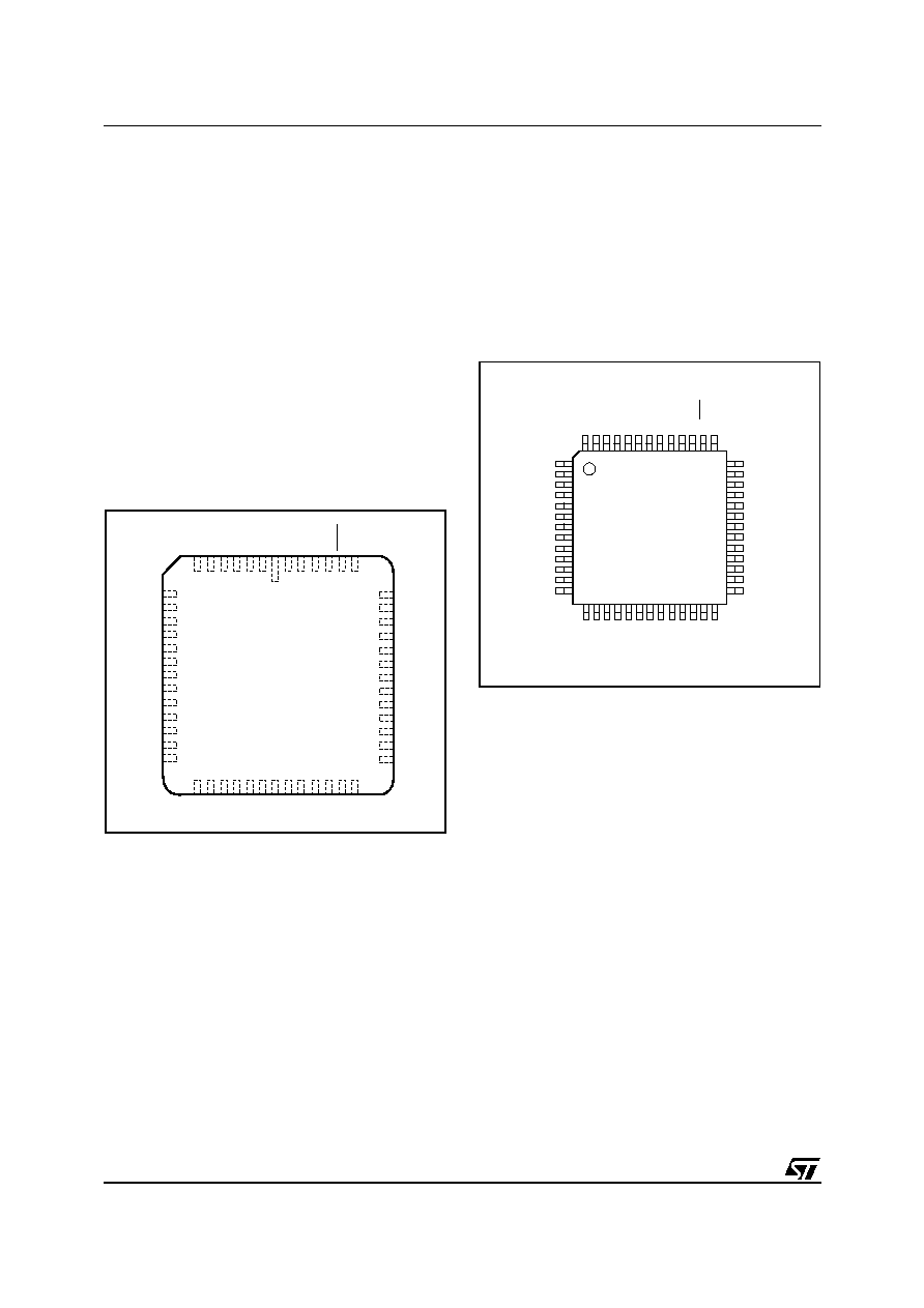
Figure 2. PLCC Connections
JTAG In-System Programming (ISP) reduces de-
velopment time, simplifies manufacturing flow,
and lowers the cost of field upgrades. The JTAG
ISP interface eliminates the need for sockets and
pre-programmed memory and logic devices. For
manufacturing, end products may be assembled
with a blank DSM device soldered to the circuit
board and programmed at the end of the manufac-
turing line in 10 to 20 seconds with no involvement
of the DSP. This allows efficient means to test
product and manage inventory by rapidly pro-
gramming test code, then application code as de-
termined by inventory requirements (Just-In Time
inventory). Additionally, JTAG ISP reduces devel-
opment time by turning fast iterations of DSP code
in the lab. Code updates in the field require no dis-
assembly of product. The FlashLINK
TM
JTAG pro-
gramming cable costs $59 USD and plugs into any
PC or note-book parallel port.
Figure 3. PQFP Connections
In addition to ISP Flash memory, DSM devices
add programmable logic (PLD) and up to 16 con-
figurable I/O pins to the DSP system. The state of
each I/O pin can be driven by DSP software or
PLD logic. PLD and I/O configuration are program-
mable by JTAG ISP, just like the Flash memory.
The PLD consists of more than 3000 gates and
has 16 macro cell registers. Common uses for the
PLD include chip selects for external devices (i.e.
UART), state-machines, simple shifters and
counters, keypad and control panel interfaces,
clock dividers, handshake delay, muxes, etc. This
eliminates the need for small external PLDs and
logic devices. Configuration of PLD, I/O, and Flash
memory mapping are easily entered in a point-
and-click environment using the software develop-
ment tool, PSDsoft Express
TM
. This software is
available at no charge from www.psdst.com.
PB0
PB1
PB2
PB3
PB4
PB5
GND
PB6
PB7
CNTL1
CNTL2
RESET
CNTL0
PA
7
PA
6
PA
5
PA
4
PA
3
GND
PA
2
PA
1
PA
0
AD0
AD1
AD2
AD3
AD15
AD14
AD13
AD12
AD11
AD10
AD9
AD8
VCC
AD7
AD6
AD5
AD4
PD2
PD1
PD0
PC7
PC6
PC5
PC4
VCC
GND
PC3
PC2
PC1
PC0
8
9
10
11
12
13
14
15
16
17
18
19
20
46
45
44
43
42
41
40
39
38
37
36
35
34
21
22
23
24
25
26
27
28
29
30
31
32
33
47
48
49
50
51
52
1
2
3
4
5
6
7
AI02857
39 AD15
38 AD14
37 AD13
36 AD12
35 AD11
34 AD10
33 AD9
32 AD8
31 V
CC
30 AD7
29 AD6
28 AD5
27 AD4
PD2
PD1
PD0
PC7
PC6
PC5
PC4
V
CC
GND
PC3
PC2
PC1
PC0
1
2
3
4
5
6
7
8
9
10
11
12
13
52
51
50
49
48
47
46
45
44
43
42
41
40
PB0
PB1
PB2
PB3
PB4
PB5
GND
PB6
PB7
CNTL1
CNTL2
RESET
CNTLO
14
15
16
17
18
19
20
21
22
23
24
25
26
PA7
PA6
PA5
PA4
PA3
GND
PA2
PA1
PA0
AD0
AD1
AD2
AD3
AI02858

5/63
DSM2180F3
Figure 4. System Block Diagram, Two-Chip Solution
The two-chip combination of a DSP and a DSM
device is ideal for systems which have limitations
on size, EMI levels, and power consumption. DSM
memory and logic are "zero-power", meaning they
automatically go to standby between memory ac-
cesses or logic input changes, producing low ac-
tive and standby current consumption, which is
ideal for battery powered products.
AI04910
ADDR & DECODE LOGIC
FLASH MEMORY
128k X 8
16 MACROCELL PLD
I/O CONTROL
POWER MANAGEMENT
CONTENT SECURITY
8 I/O
PORTS
8 I/O
PORTS
JTAG
ISP TO
ALL
AREAS
I/O BUS
MEM PAGE CONTROL
22 ADDRESS
8 DATA
WR, RD, BMS, DMS, IOMS
I/O, PLD, CHIP SELECTS
ISP, I/O, PLD, CHIP SEL
DSM2180F3
DSP SYSTEM MEMORY
ANALOG
DEVICES
DSP
ADSP-218X
FAMILY
SERIAL
DEVICE
SERIAL
DEVICE
13 FLAGS / 4 INTR