Rev 1
August 2005
1/12
12
DVIULC6-4SC6
Ultra low capacitance ESD protection
Main applications
DVI ports up to 1.65 Gb/s
HDMI ports up to 1.65 Gb/s
IEEE 1394a and IEEE 1394b ports up to
1.6 Gb/s
USB2.0 ports up to 480 Mb/s (high speed),
backwards compatible with USB1.1 low and full
speed
Ethernet port: 10/100/1000 Mb/s
SIM card protection
Video line protection
Description
The DVIULC6-4SC6 is a monolithic, application
specific discrete device dedicated to ESD
protection of high speed interfaces, such as DVI,
HDMI, IEEE 1394a and IEEE 1394b, USB2.0,
Ethernet links and video lines.
Its ultra low line capacitance secures a high level
of signal integrity without compromising in
protecting sensitive chips against the most
stringent characterized ESD strikes.
Features
4 line ESD protection
Protects V
BUS
when applicable
Ultra low capacitance: 0.6 pF at F = 825 MHz
Fast response time
SOT23-6L package
RoHS compliant
Order code
Complies with these standards:
IEC61000-4-2 level 4
� 15 kV (air discharge)
� 8 kV (contact discharge)
Benefits
ESD standards compliance guaranteed at
device level, hence greater immunity at system
level
ESD protection of V
BUS
when applicable.
Allows ESD current flowing to Ground when
ESD event occurs on data line
Optimized rise and fall times for maximum data
integrity
Consistent D+ / D- signal balance:
� Best capacitance matching tolerance I/O to
GND = 0.015 pF for ultra low inter pair skew
� Best capacitance matching tolerance I/O to
I/O = 0.007 pF for ultra low intra pair skew
� Matching high bit rate DVI, HDMI, and
IEEE 1394 requirements
Low PCB space consuming, 9mm� maximum
foot print
Low leakage current for longer operation of
battery powered devices
Higher reliability offered by monolithic
integration
Part Number
Marking
DVIULC6-4SC6
DL46
SOT23-6L
(JEDEC MO178AB)
www.st.com

DVIULC6-4SC6
2/12
Figure 1.
Functional Diagram
Table 1.
Absolute Ratings
Symbol
Parameter
Value
Unit
V
PP
Peak pulse voltage
At device level:
IEC61000-4-2 air discharge
IEC61000-4-2 contact discharge
MIL STD883C-Method 3015-6
�15
�15
�25
kV
T
stg
Storage temperature range
-55 to +150
�C
T
j
Maximum junction temperature
125
�C
T
L
Lead solder temperature (10 seconds duration)
260
�C
Table 2.
Electrical Characteristics (T
amb
= 25�C)
Symbol
Parameter
Test Conditions
Value
Unit
Min.
Typ.
Max
I
RM
Leakage current
V
RM
= 5 V
0.5
�A
V
BR
Breakdown voltage between V
BUS
and GND I
R
= 1 mA
6
V
V
CL
Clamping voltage
I
PP
= 1 A, t
p
= 8/20 �s
Any I/O pin to GND
12
V
I
PP
= 5 A, t
p
= 8/20 �s
Any I/O pin to GND
17
V
C
i/o-GND
Capacitance between I/O and GND
V
R
= 0 V, F= 1 MHz
0.85
1
pF
V
R
= 0 V, F= 825 MHz
0.6
C
i/o-GND
Capacitance variation between I/O and GND
0.015
C
i/o-i/o
Capacitance between I/O
V
R
= 0 V, F= 1 MHz
0.42
0.5
pF
V
R
= 0 V, F= 825 MHz
0.3
C
i/o-i/o
Capacitance variation between I/O
0.007
1
1
6
2
5
3
4
I/O1
I/O4
GND
V
BUS
I/O2
I/O3

1 Surge protection
DVIULC6-4SC6
4/12
Technical information
1 Surge
protection
The DVIULC6-4SC6 is particularly optimized to perform ESD surge protection based on the rail
to rail topology.
The clamping voltage V
CL
can be calculated as follow:
with: V
F
= V
T
+ R
d
.I
p
(V
F
forward drop voltage) / (V
T
forward drop threshold voltage)
We assume that the value of the dynamic resistance of the clamping diode is typically:
R
d
= 1.4
and V
T
= 1.2 V.
For an IEC61000-4-2 surge Level 4 (Contact Discharge: V
g
=8 kV, R
g
=330
), V
BUS
= +5 V, and
if in first approximation, we assume that: I
p
= V
g
/ R
g
= 24 A.
So, we find:
Note:
The calculations do not take into account phenomena due to parasitic inductances.
V
CL
+ = V
BUS
+ V
F
for positive surges
V
CL
- = - V
F
for
negative
surges
V
CL
+ = +39 V
V
CL
- = -34 V
DVIULC6-4SC6
2 Surge protection application example
5/12
2
Surge protection application example
If we consider that the connections from the pin V
BUS
to V
CC
and from GND to PCB GND are
done by two tracks of 10mm long and 0.5 mm large; we assume that the parasitic inductances
L
w
of these tracks are about 6nH. So when an IEC61000-4-2 surge occurs, due to the rise time
of this spike (tr=1 ns), the voltage V
CL
has an extra value equal to Lw.dI/dt.
The dI/dt is calculated as: dI/dt = Ip/tr = 24 A/ns
The over voltage due to the parasitic inductances is: Lw.dI/dt = 6 x 24 = 144 V
By taking into account the effect of these parasitic inductances due to unsuitable layout, the
clamping voltage will be:
We can reduce as much as possible these phenomena with simple layout optimization.
It's the reason why some recommendations have to be followed (see
Section 3: How to ensure
a good ESD protection
).
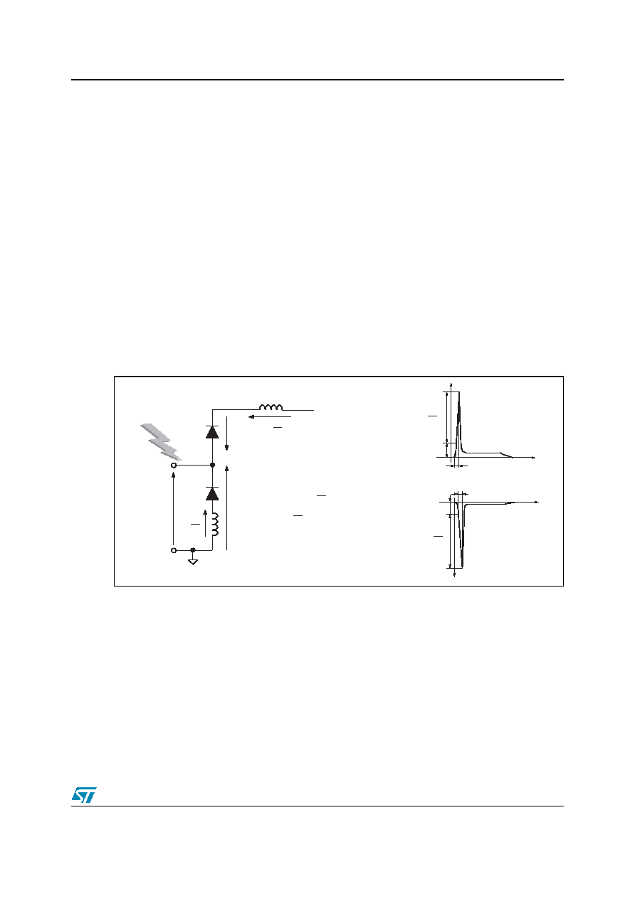
Figure 6.
ESD behavior: parasitic phenomena due to unsuitable layout
V
CL
+ = +39 + 144 = 183 V
V
CL
- = -34 - 144 = -178 V
Lw
VI/O
ESD
SURGE
GND
I/O
+V
CC
V
BUS
V
F
Lw di
dt
Lw di
dt
V
+ =
CL
V
+V +Lw
BUS
F
di
dt
surge >0
di
dt
surge <0
V
- =
CL
-V -Lw
F
t
tr=1ns
V
V
CC
F
+
Lw
di
dt
V
CL+
POSITIVE
SURGE
183V
-Lw
di
dt
t
tr=1ns
-
V
F
V
CL-
NEGATIVE
SURGE
-178V
