 | –≠–ª–µ–∫—Ç—Ä–æ–Ω–Ω—ã–π –∫–æ–º–ø–æ–Ω–µ–Ω—Ç: EF9345 | –°–∫–∞—á–∞—Ç—å:  PDF PDF  ZIP ZIP |
EF9345
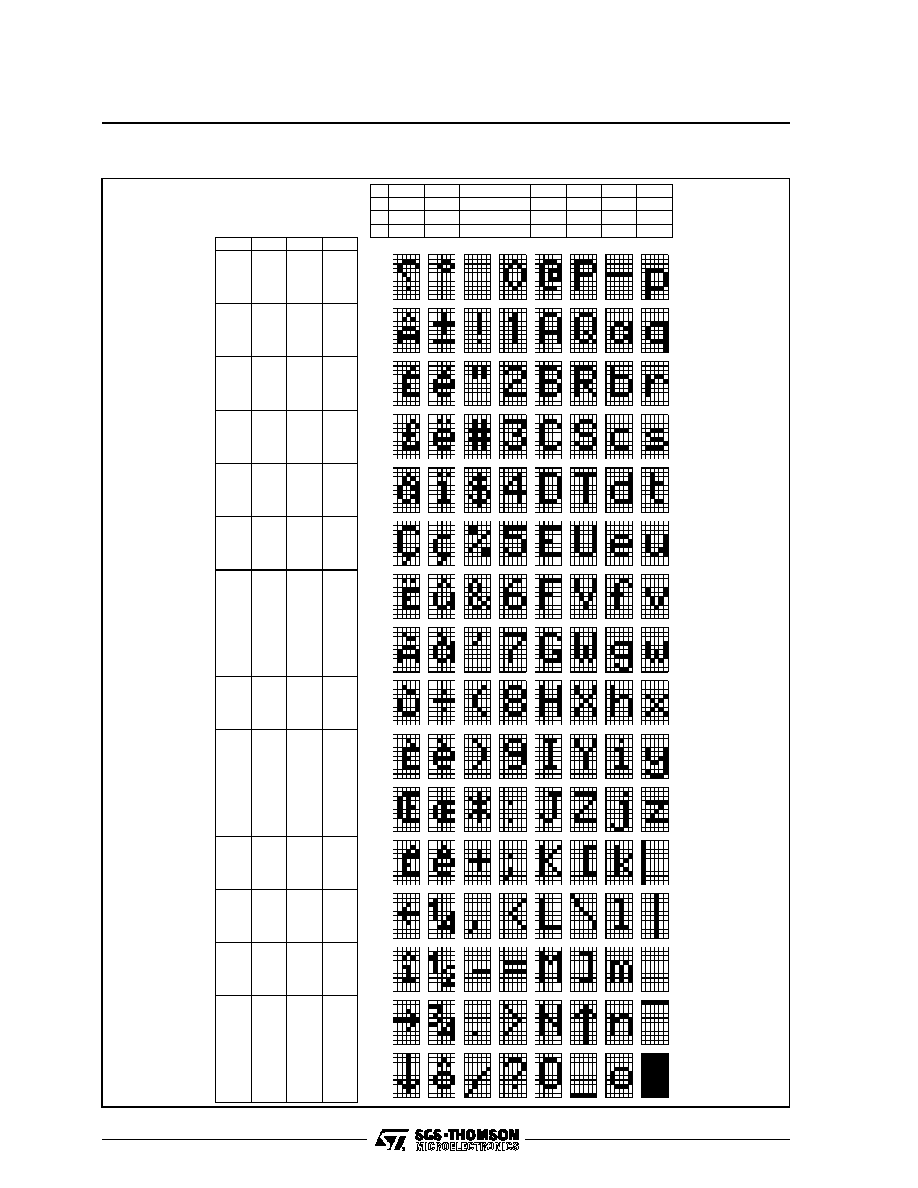
HMOS2 SINGLE CHIP SEMI-GRAPHIC
DISPLAY PROCESSOR
March 1995
DIP40
(Plastic Package)
ORDER CODE : EF9345P
.
SINGLE CHIP LOW-COST COLOR CRT
CONTROLLER
.
TV STANDARD COMPATIBLE (50Hz or 60Hz)
.
2 SCREEN FORMATS :
- 25 (or 21) ROWS OF 40 CHARACTERS
- 25 (or 21) ROWS OF 80 CHARACTERS
.
ON-CHIP 128 ALPHANUMERIC AND 128
SEMI-GRAPHIC CHARACTER GENERATOR
TWO STANDARD OPTIONS AVAILABLE FOR
ALPHANUMERIC SETS (EF9345-R003 IS NO
MORE AVAILABLE)
.
EASY EXTENSION OF USER DEFINED AL-
PHANUMERIC OR SEMI-GRAPHIC SETS
(> 1 K CHARACTERS)
.
40 CHARACTERS/ROW ATTRIBUTES : FORE-
GROUND AND BACKGROUND COLOR, DOU-
BLE HEIGHT, DOUBLE WIDTH, BLINKING,
REVERSE, UNDERLINING, CONCEAL, IN-
SERT, ACCENTUATION OF LOWER CASE
CHARACTERS
.
80 CHARACTERS/ROW ATTRIBUTES : UN-
DERLINING, BLINKING, REVERSE, COLOR
SELECT
.
PROGRAMMABLE ROLL-UP, ROLL-DOWN
AND CURSOR DISPLAY
.
ON-CHIP R, G, B, I VIDEO SHIFT REGISTERS
.
EASY SYNCHRONIZATION WITH EXTER-
NAL VIDEO-SOURCE : ON-CHIP PHASE
COMPARATOR
.
ADDRESS/DATA MULTIPLEXED
BUS
DI-
RECTLY COMPATIBLE WITH STANDARD MI-
CROCOMPUTERS SUCH AS 6801, 6301,
8048, 8051, ST9
.
ADDRESSING SPACE : 16K x 8 OF GEN-
ERAL PURPOSE PRIVATE MEMORY
.
EASY OF USE OF ANY LOW-COST MEM-
ORY COMPONENTS : ROM, SRAM, DRAM
DESCRIPTION
The EF9345, new advanced color CRT controller,
in conjunction with an additional standard memory
package allow full implementation of the complete
display control unit of a color or monochrome low-
cost termainl, thus significantly reducing IC cost
and PCB space.
1
2
3
4
5
6
7
8
9
10
11
12
40
39
38
37
36
35
34
33
32
31
30
29
28
27
26
25
13
14
15
16
17
18
19
20
24
23
22
21
OE
WE
ASM
HVS/HS
PC/VS
B
G
R
I
HP
CLK
SYNC IN
AS
DS
R/W
AD0
AD1
AD2
V
SS
V
CC
ADM0
ADM1
ADM2
ADM3
ADM4
ADM5
ADM6
ADM7
AM8
AM9
AM10
AM11
AM12
AM13
CS
AD7
AD6
AD5
AD4
AD3
9345-01.EPS
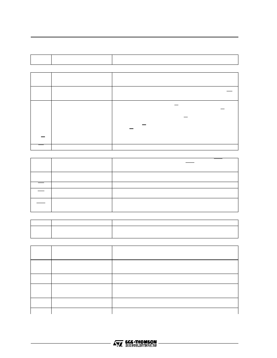
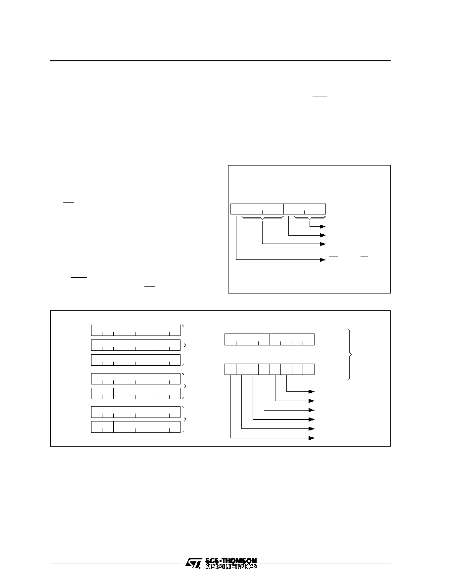
PIN CONNECTIONS
1/38
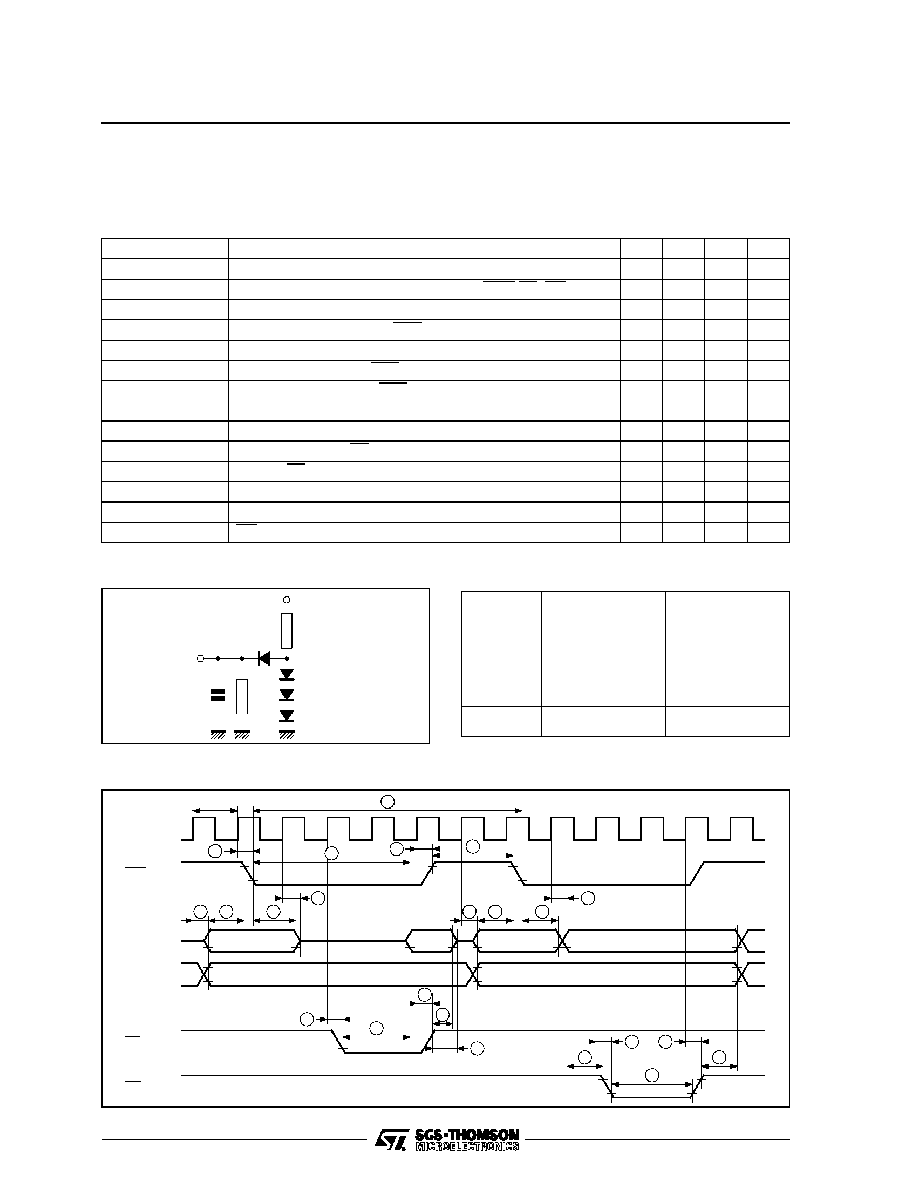
PIN DESCRIPTION (All the input/output pins are TTL compatible)
Name
Pin
Type
Pin N
∞
Function
Description
MICROPROCESSOR INTERFACE
AD(0:7)
I/O
17-29
21-25
Multiplexed
Address/Data
Bus
These 8 bidirectional pins provide communication with the
microprocessor system bus.
AS
I
14
Address
Strobe
The falling edge of this control signal latches the address on the
AD(0:7) lines, the state of the Data Strobe (DS) and Chip Select (CS)
into the chip.
DS
I
15
Data Strobe
When this input is strobed high by AS, the output buffers are selected
while DS is low for a read cycle (R/W = 1).
In write cycle, data present on AD(0:7) lines are strobed by R/W low
(see timing diagram 2).
When this input is strobed low by AS, R/W gives the direction of data
transfer on AD(0:7) bus. DS high strobes the data to be written during
a write cycle (R/W = 0) or enables the output buffers during a read
cycle (R/W = 1). (see timing diagram 1).
R/W
I
16
Read/Write
This input determines whether the Internal registers get written or
read. A write is active low ("O").
CS
I
26
Chip Select
The EF9345 is selected when this input is strobed low by AS.
MEMORY INTERFACE
ADM(0:7)
I/O
40-43
Multiplexed
Address/Data
Bus
Lower 8 bits of memory address appear on the bus when ASM is
high. It then becomes the data bus when ASM is low.
AM(8:13)
O
32-27
Memory
Address Bus
These 6 pins provide the high order bits of the memory address.
OE
O
2
Output Enable
When low, this output selects the memory data output buffers.
WE
O
3
Write Enable
This output determines whether the memory gets read or written. A
write is active low ("0").
ASM
O
4
Memory
Address
Strobe
This signal cycles continuously. Address can be latched on its falling
edge.
OTHER PINS
CLK
I
12
Clock Input
External TTL clock Input (nominal value : 12MHz, duty cycle : 50%).
V
SS
S
1
Power Supply
Ground.
V
CC
S
20
Power Supply
+5V
VIDEO INTERFACE
R
G
B
O
O
O
7
8
9
Red
Green
Blue
These outputs deliver the video signal. They are low during the
vertical and horizontal blanking intervals.
I
O
10
Insert
This active high output allows to insert R : G: B : in an external video
signal for captioning purposes, for example. It can also be used as a
general purpose attribute or color.
HVS/HS
O
5
Sync. Out
This output delivers either the composite synchro (bit TGS
4
= 1) or the
horizontal synchro signal (bit TGS
4
= 0)
PC/VS
O
6
Phase
Comparator /
Vertical Sync
When TGS
4
= 1, this signal is the phase comparator output.
When TGS
4
= 0, this output delivers the vertical synchro signal.
SYNC IN
I
13
Synchro In
This input allows vertical and/or horizontal synchronizing the EF9345
on an external signal. It must be grounded if not used.
HP
O
11
Video Clock
This output delivers a 4MHz clock phased with the R, G, B, I signals.
9345-01.TBL
EF9345
2/38
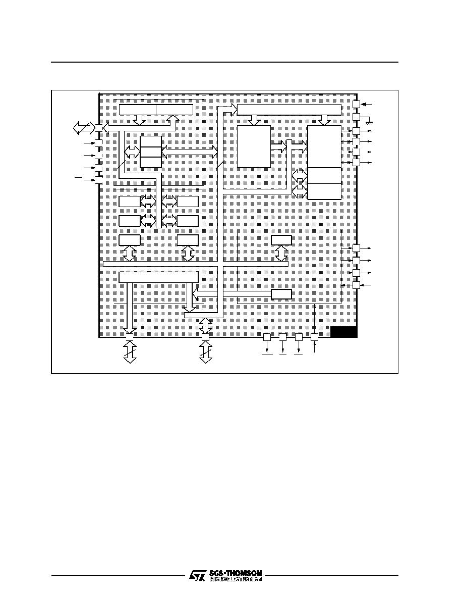
ADDRESS UNIT
6
AM(8:13)
8
AD M(0:7)
8
AD(0:7)
STA
CMD
R1
R2
8
MPU ACCESS
R3
R5
R3
ROR
R3
TRANSCODER
R3
R6
R3
R4
R3
R7
R3
DOR
16
CS
14
AS
15
DS
16
R/W
DATA
BUS
ROM
R3
TSG
TIMING
GENERATOR
R3
RFSH
ROW BUFFER 120 x 8
ATTRIBUTE
LOGIC
MAT
PAT
+5V
R
G
B
I
9
8
7
10
13
11
5
6
HP
HVS/HS
PC/VS
SYNC. IN
3
WE
2
OE
4
ASM
12
CLK
5
6
8
R3
EF9345
9345-02.EPS
BLOCK DIAGRAM
EF9345
3/38
ABSOLUTE MAXIMUM RATINGS
Symbol
Parameter
Value
Unit
V
CC
*
Supply Voltage
-0.3, 7.0
V
V
in
*
Input Voltage
-0.3, 7.0
V
T
A
Operating Temperature
0, +70
o
C
T
stg
Storage Temperature
-55, +150
o
C
P
Dm
Maximum Power Dissipation
0.75
W
* With respect to Vss.
Stresses above those hereby listed may cause permanent damage to the device. The ratings are stress ones only and functional operation of
the device at these or any conditions beyond those indicated in the operational sections of this specification is not implied. Exposure to maximum
rating conditions for extended periods may affect reliability. Standard MOS circuits handling procedure should be used to avoid possible damage
to the device.
9345-02.TBL
ELECTRICAL CHARACTERISTICS
V
CC
= 5.0V
±
5%, V
SS
= 0V, T
A
= 0 to +70
∞
C, unless otherwise specified.
Symbol
Parameter
Min.
Typ.
Max.
Unit
V
CC
Supply Voltage
4.75
5
5.25
V
V
IL
Input Low Voltage
-0.3
0.8
V
V
IH
Input High Voltage :
CLK
Other Inputs
2.2
2
V
CC
V
CC
V
I
IN
Input Leakage Current
10
µ
A
V
OH
Output High Voltage (I
loa d
= -500
µ
A)
2.4
V
V
OL
Output Low Voltage : I
load
= 4mA ; AD(0:7), ADM(0:7), AM(8:13)
I
load
= 1mA ; Other Outputs
0.4
0.4
V
P
D
Power Dissipation
250
mW
C
IN
Input Capacitance
15
pF
I
TSI
Three State (Off State) Input Current
10
µ
A
9345-03.TBL
EF9345
4/38
MEMORY INTERFACE
V
CC
= 5.0V
±
5%, T
A
= 0 to + 70
∞
C
Clock : f
in
= 12MHz ; Duty Cycle 40 to 60% ; t
r
, t
f
< 5ns
Reference Levels : V
IL
= 0.8V and V
IH
= 2V, V
OL
= 0.4V and V
OH
= 2.4V
Symbol
Ident. N
∞
Parameter
Min.
Typ.
Max.
Unit
t
ELEL
1
Memory Cycle Time
500
ns
t
D
2
Output Delay Time from CLK Rising Edge (ASM, OE, WE)
60
ns
t
EHEL
3
ASM High Pule Width
120
ns
t
ELDV
4
Memory Access Time from ASM Low
290
ns
t
DA
5
Output Delay Time from CLK Rising Edge (ADM(0:7), AM(8:13))
80
ns
t
AVEL
6
Address Setup Time to ASM
30
ns
t
ELAX
7
Address Hold Time from ASM
55
ns
t
CLAZ
8
Address Off Time
80
ns
t
GHDX
9
Memory Hold Time
10
ns
t
OZ
10
Data Off Time from OE
60
ns
t
GLDV
11
Memory OE Access Time
150
ns
t
QVWL
12
Data Setup Time (Write Cycle)
30
ns
t
WHQX
13
Data Hold Time (Write Cycle)
30
ns
t
WLWH
14
WE Pulse Width
110
ns
9345-04.TBL
V
DD
R
C
L
Test
Point
R
L
MMD7000
or equivalent
9345-03.EPS
Figure 1 : Test Load
Table 1
Symbol
AM(8:13)
ADM(0:7)
AD(0:7)
Other
Outputs
C
100pF
50pF
R
L
1k
3.3k
R
4.7k
4.7k
9345-05.TBL
READ ADDRESS
WRITE ADDRESS
D
IN
D
OUT
CLK
ASM
ADM (0:7)
AM (8:14)
OE
WE
T
1
2
3
4
5
6
7
8
9
10
11
12
13
14
5
6
7
5
2
2
2
2
2
9345-04.EPS
Figure 2 : Memory Interface Timing Diagram
EF9345
5/38
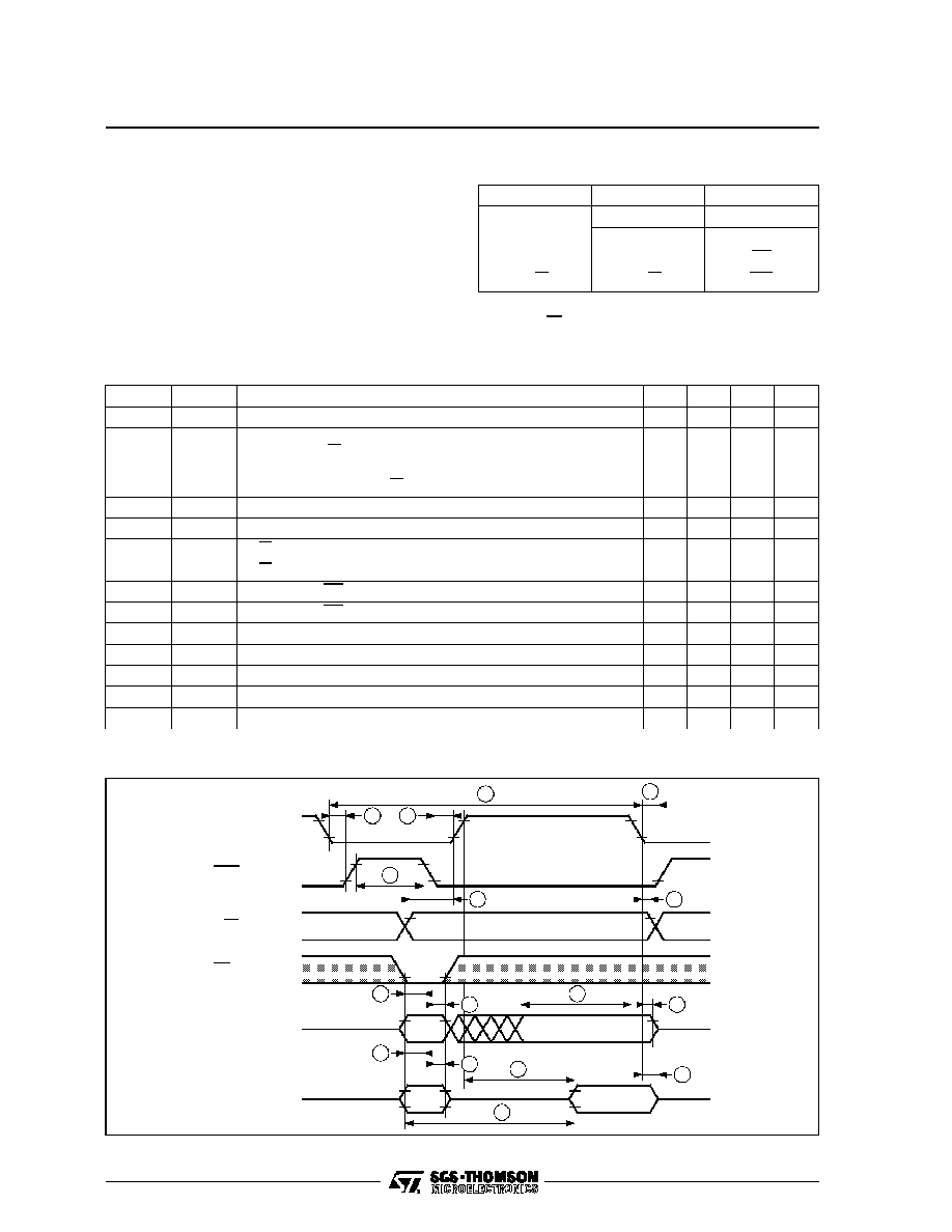
MICROPROCESSOR INTERFACE
EF9345 is motel compatible. It automatically se-
lects the processor type by using AS input latch to
state of the DS input.
No external logic is needed to adapt bus control
signals from most of the common multiplexed bus
microprocessors.
EF9345
6801
INTEL Family
Timing 1
Timing 2
AS
AS
ALE
DS
DS, E,
2
RD
R/W
R/W
WR
MICROPROCESSOR INTERFACE TIMING AD(0:7), AS, DS, R/W, CS
V
CC
= 5.0V
±
5%, T
A
= 0 to + 70
∞
C, C
L
= 100pF on AD(0:7)
Reference Levels : V
IL
= 0.8V and V
IH
= 2V on All Inputs ; V
OL
= 0.4V and V
OH
on all Outputs.
Symbol
Ident. N
∞
Parameter
Min.
Typ.
Max.
Unit
t
CYC
1
Memory Cycle Time
400
ns
t
ASD
2
DS Low to AS High (Timing 1)
DS High or R/W High to AS High (Timing 2)
30
ns
t
ASED
3
AS Low to High (Timing 1)
AS Low to DS Low or R/W Low (Timing 2)
30
ns
t
PWEH
4
Write Pulse Width
200
ns
t
PWASH
5
AS Pulse Width
100
ns
t
RWS
6
R/W to DS Setup Time (Timing 1)
100
ns
t
RWH
7
R/W to DS Hold Time (Timing 1)
10
ns
t
ASL
8
Address and CS Setup Time
20
ns
t
AHL
9
Address and CS Hold Time
20
ns
t
DSW
10
Data Setup Time (Write Cycle)
100
ns
t
DHW
11
Data Hold Time (Write Cycle)
10
ns
t
DDR
12
Data Access Time from DS (Read Cycle)
150
ns
t
DHR
13
DS Inactive to High Impedance State Time (Read Cycle)
10
80
ns
t
ACC
14
Address to Data Valid Access Time
300
ns
9345-06.TBL
1
2
3
5
7
8
9
10
11
12
13
14
INPUT DATA
OUTPUT
DATA
2
8
9
ADDRESS
ADDRESS
6
DS
ASM
R/W
CS
WRITE CYCLE
AD (0:7)
READ CYCLE
AD (0:7)
9345-05.EPS
Figure 3 : Microprocessor Interface Timing Diagram 1 (6801 Type)
EF9345
6/38
ADDRESS
1
2
3
5
8
9
2
ALE
(Pin AS)
RD
(Pin DS)
WR
(Pin R/W)
CS
AD(0:7)
4
D
IN
10
11
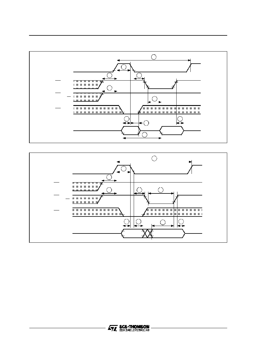
9345-07.EPS
Figure 5 : Microprocessor Interface Timing Diagram 2 (INTEL Type) - Write Cycle
ADDRESS
D
OUT
1
2
3
5
8
9
12
13
14
2
ALE
(Pin AS)
RD
(Pin DS)
WR
(Pin R/W)
CS
AD(0:7)
9345-06.EPS
Figure 4 : Microprocessor Interface Timing Diagram 2 (INTEL Type) - Read Cycle
EF9345
7/38
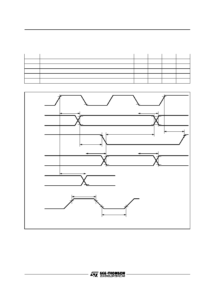
VIDEO INTERFACE R, G, B, I, HP, HVS/HS, PC/VS
V
CC
= 5.0V
±
5%, T
A
= 0 to + 70
∞
C, CLK Duty Cycle = 50%, C
L
= 50pF
Reference Levels : V
IL
= 0.8V and V
IH
= 2.2V on CLK Inputs. V
OL
= 0.4V and V
OH
= 2.4V on all Outputs.
Symbol
Parameter
Min.
Typ.
Max.
Unit
t
SU
Setup Time R, G, B, I to HP
10
ns
t
HO
Hold Time R, G, B, I from HP
50
ns
t
D
Output Delay from CLK Edge
60
ns
t
PWCH
CLK High Pulse Width
30
ns
t
PWCL
CLK Low Pulse Width
30
ns
9345-07.TBL
CLK
R, G, B, I,
40 char/row
R, G, B, I,
80 char/row
HVS/HS
PC/VS
t
D
t
D
t
D
t
D
t
D
CLK
t
PWCH
t
PWCL
HP
t
SU
t
HO
t
D
INPUT CLK
9345-08.EPS
Figure 6
EF9345
8/38
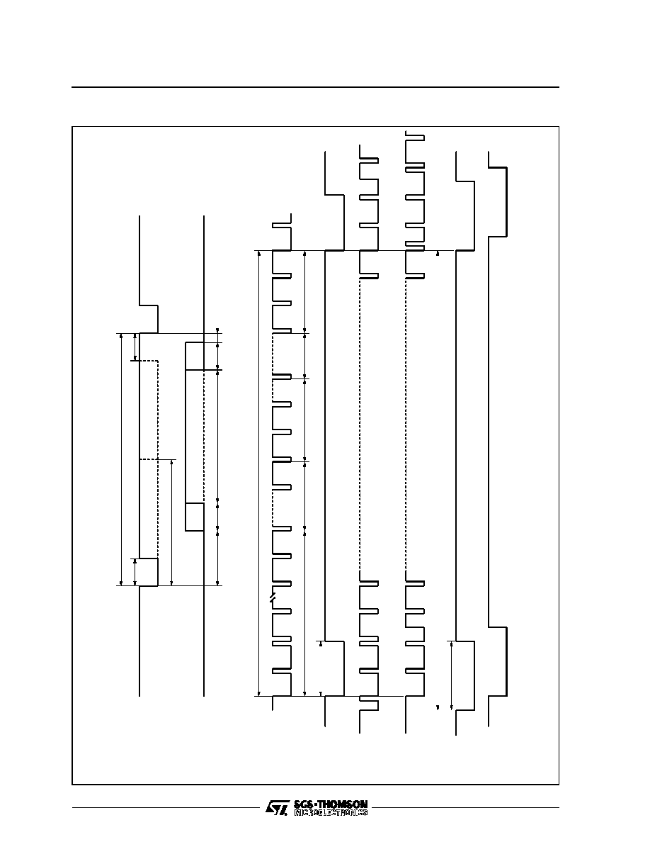
2.5
lines
312.5
lines
(TGS
0
=0
)
Even
Frame
Odd
Frame
Even
Frame
312
lines
(TGS
0
=0
)
Blanking
25
Lines
Margin
16
Lines
Page
250
Lines
Margin
18
Lines
Blanking
3
Lines
V
OH
V
OL
HVS
(TGS
4
=1
)
NON
INTERLACED
INTERLACED
V
E
R
T
I
CAL
S
Y
NCHRO
H
O
RI
Z
O
NT
AL
S
Y
N
CHRO
4.5
µ
s
4.5
µ
s
64
µ
s
32
µ
s
Odd
frame
1/2
pulse
Even
frame
1/2
pulse
HVS
Bulk
40
µ
s6
µ
s2
µ
s
2.04
µ
s
10
µ
s
9.96
µ
s
Margin
Margin
H
Blanking
H
Blanking
40
µ
s6
µ
s
6
µ
s
6
µ
s
40
char/row
80
char/row
R,
G,
B,
I
2
lines
VS
(TGS
4
=0
)
HVS
(TGS
4
=1
)
VS
(TGS
4
=0
)
Odd
Frame
362.5
lines
(TGS
0
=1
)
TGS
0
=0
TGS
0
=
1
25
Lines
10
Lines
210
Lines
14
Lines
3
Lines
362
lines
(TGS
0
=1
)
9345-09.EPS
Figure 7 : Vertical and Horizontal Synchronization Outputs (CLK = 12MHz)
EF9345
9/38

FUNCTIONAL DESCRIPTION
The EF9345 is a low cost, semigraphic, CRT con-
troller.
It is optimized for use with a low cost, monochrome
or color TV type CRT (64ms per line, 50 or 60Hz
refresh frequency).
The EF9345 displays up to 25 rows of 40 charac-
ters or 25 rows of 80 characters.
The on-chip character generator provides a 128
standard, 5 x 7, character set and standard semi-
graphic sets.
More use definable (8 x 10) alphanumeric or semi-
graphic sets may be mapped in the 16 K x 8 private
memory addressing space.
These user definable sets are available only in 40
characters per row format.
Microprocessor Interface
The EF9345 provides an 8-bit, adress/data multi-
plexed microprocessor interface.
It is directly compatible with popular (6801, 8048,
8051, 8035, ...) microprocessors.
Registers
The microprocessor directly accesses 8 registers :
- R0 : Command/status register.
- R1, R2, R3 : Data registers.
- R4, R5, R6, R7 : Each of these register pairs
points into the private memory.
Through these registers, the microprocessor indi-
rectly accesses the private memory and 5 more
registers :
- ROR, DOR : Base address of displayed page
memory and used external character generators.
- PAT, MAT, TGS : Used to select the page attrib-
utes and format, and to program the timing gen-
erator option.
Private Memory
The user may partition the 16 K x 8 private memory
addressing space between :
- Page of character codes (2 K x 8 or 3 K x 8),
- External character generators,
- General purpose user area.
Many types of memory components are suitable :
- ROM, DRAM or SRAM,
- 2 K x 8, 8 K x 8, 16 K x 4 organizations,
- Modest 500ns cycle time and 250ns access time
is required.
40 Characters per Row : Character Code
Formats and Attributes
Once the 40 characters per row format has been
selected, one character code format out of three
must be chosen :
- 24-bit fixed format :
All the attributes are provided in parallel.
- 8/24-bit compressed format :
All the attributes are latched.
- 16-bit fixed format :
Some parallel attributes, other are latched.
Character attributes provided :
- Background and foreground color (3 bits each),
- Double height, double width,
- Blinking,
- Reverse,
- Underlining,
- Conceal,
- Insert,
- Accentuation of lower case characters,
- 3 x 100 user definable character generator in
memory,
- 8 x 100 semi-graphic quadrichrome characters.
80 Characters per Row Format : Character
Code Format and Attributes
Two character code formats are provided :
- Long (12 bits) with 4 parallel attributes :
∑
Blinking,
∑
Underlining,
∑
Reverse,
∑
Color select.
- Short (8 bits) : no attributes.
Timing Generator
The whole timing is derived from a 12MHz main
clock input.
The RGB outputs are shifted at 8MHz for the 40
character/row format and at 12MHz for the 80
character/row.
Besides, the user may select :
- 50Hz or 60Hz vertical sync. frequency,
- Interlaced or not,
- Separated or composite vertical and horizontal
sync. ouputs.
Furthermore, a composite sync. input allows, when
it is required :
- An on-chip vertical resynchronization,
- An on-chip crude horizontal resynchronization,
- An off-chip high performance horizontal resyn-
chronization by use of a simple external VCXO
controlled by the on-chip phase comparator.
EF9345
10/38
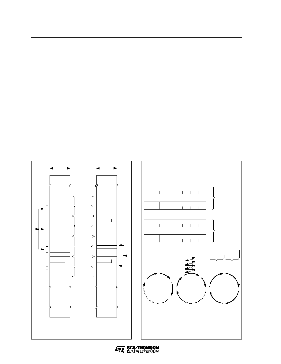
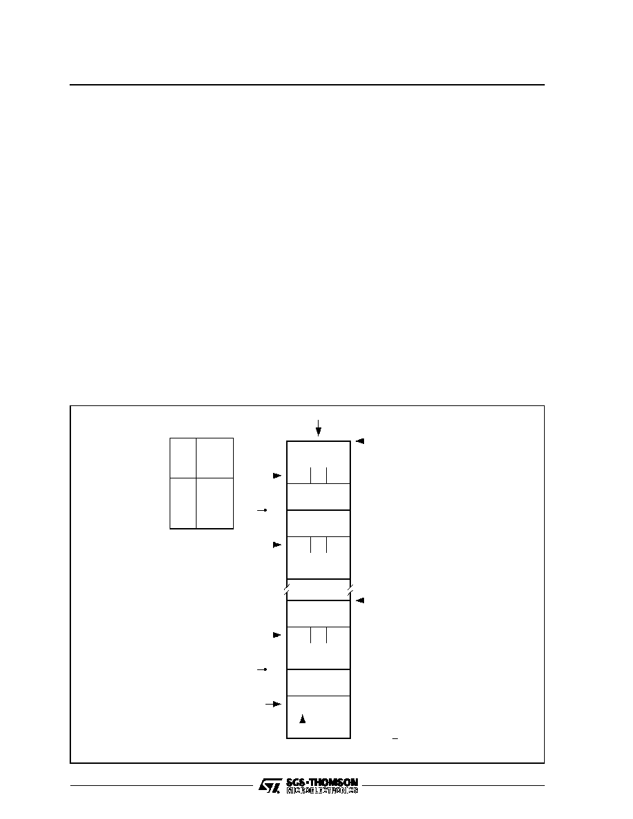
MEMORY ORGANIZATION
Logical And Physical Addressing
The physical 16-Kbyte addressingspace is logicaly
partitioned by EF9345 into 40-byte buffers (Fig-
ure 8). More precisely, a logical address is given by
an X, Y, Z triplet where :
- X = (0 to 39) points to a byte inside a buffer,
- Y = (0, 1 ; 8 to 31) points to a buffer inside a
1 Kbyte blocks,
- Z = (0 to 15) points to a block.
Obviously, 1 K = 2
10
= 1024 cannot be exactly
divided by 40. Consequently, any block holds 25
full buffers and a 24-byte remainder. Provided that
the physical memory is a multiple of 2 Kbytes, the
remainders are paired in such a way as to make
available :
- A full buffer (Y = 1) in each even block,
- A partial buffer (Y = 1 ; X = 32 to 39) in each odd
block.
DISTRICT
8
39
X
0
8
31
0
0
1
31
0
8
31
0
8
31
DISTRICT
DISTRICT
0
9
BLOCK 0
(1Kbyte)
BLOCK 1
BLOCK 2
BLOCK 3
8
39
X
Y
Y
120-BYTE ROW BUFFER
80-BYTE ROW BUFFER
- Row buffers lay indide a district
- At two or three successive block addresses (modulo 4)
- First block address is even
32
32
8
1
1
1
Notes :
9345-10.EPS
Figure 8 : Memory Row Buffer
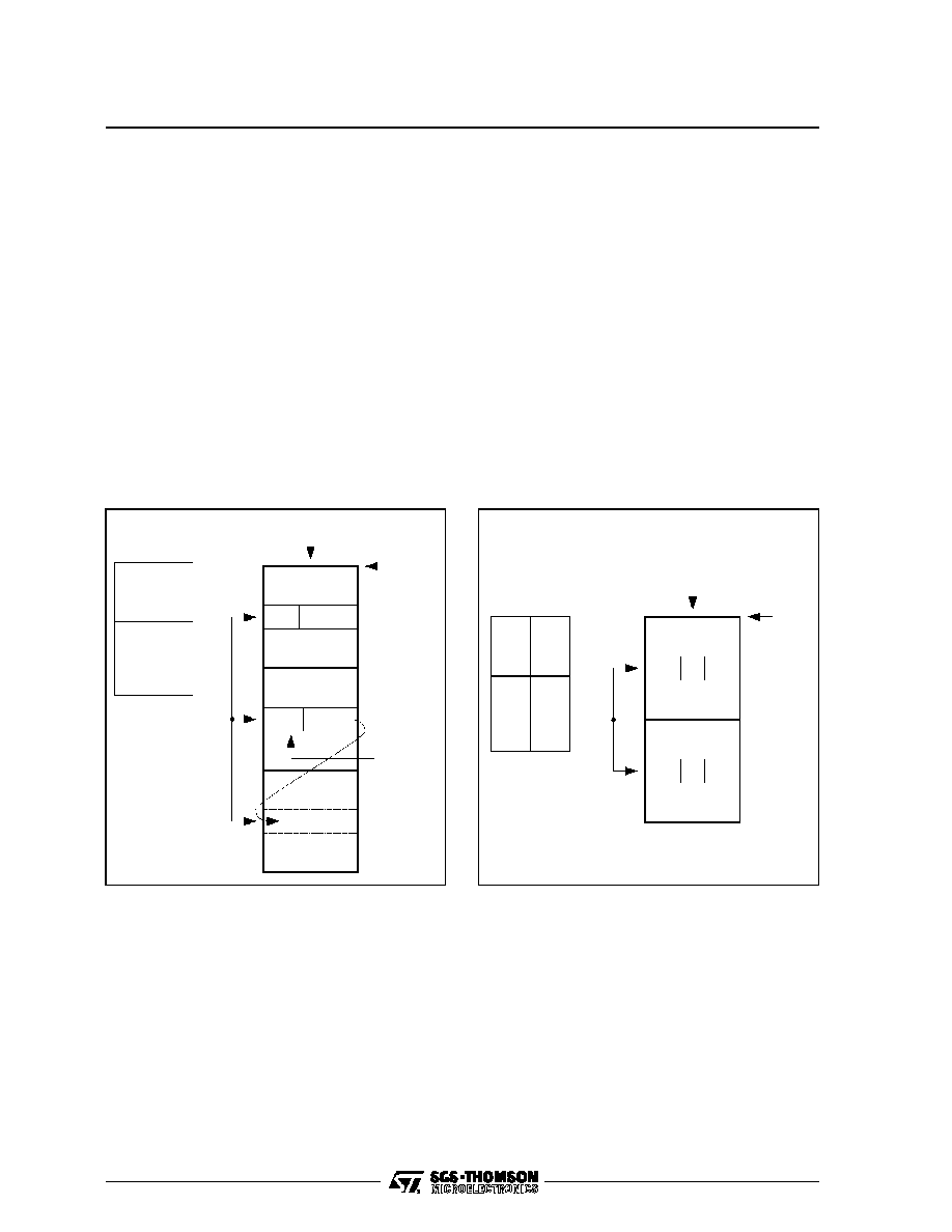
Pointers
Each X, Y and Z component of a logical address is
binary encoded and packed in two 8-bits registers.
Such a register pair is a pointer (Figure 9). EF9345
contains two pointers :
- R4, R5 : auxiliary pointer,
- R6, R7 : main pointer.
R5 and R7 have the same format. Each one holds
an X component and the two LSB's of a Z compo-
nent. This packing induces a partitioning of Z in 4
districts of 4 blocks each.
R5, R7 points to a block number in a district. R4
and R6 have a slightly different format : Each one
holds a Y component and the LSB of the district
number. But R6 holds both district MSB
Figure 11 gives the logical to physical address
transcoding scheme performed on chip.
d1
d'1
d0
4
3
2
1
0
R6
Y = (0, 1 ; 8 to 31)
b0
b1
5
4
3
2
1
0
R7
X = 0 to 39
MAIN
POINTER
_
_
d'0
4
3
2
1
0
R4
Y' = (0, 1 ; 8 to 31)
b'0
b'1
5
4
3
2
1
0
R5
X' = 0 to 39
AUXILIARY
POINTER
3
2
1
0
Z = (0 to 15)
D
B
39
1
2
0
2 = 0
4 = 0
6 = 0
1
3 = 1
5 = 1
7 = 1
X incrementation
Modulo 40
Y incrementation
Modulo 24
Z incrementation/
decrementation
Modulo 4 on the
block number only
0
X
Y
B
31
8
9
10
1
2
3
0
9345-11.EPS
Figure 9 : Pointer Auto Incrementation
EF9345
11/38
Data Structure in Memory
A page is a data structure displayable on the
screen up to 25 rows of characters. According to
the character code format, each row on the screen
is associated with 2 (or 3) 40-byte buffers. This set
of 2 (or 3) buffers constitutes a row buffer (Fig-
ure 8). The buffers belonging to a row buffer must
meet the following requirements :
- They have the same Y address,
- They have the same district number,
- They lie at 2 (or 3) successive (modulo 4) block
addresses in their common district.
Consequently, a row buffer is defined by its first
buffer address and its format.
A page is a set of successive row buffers :
- With the same format,
- With the same district number,
- With the same block address of first buffer. This
block address must be even,
- Lying at successive (modulo 24) Y addresses.
Consequently, a page should not cross a district
boundary. General purpose memory area may be
used but should respect the buffer of row buffer
structure. See Figure 9 for pointer incrementation
implied by these data structures.
Memory Time Sharing (See Figure 10)
The memory interface provides a 500 ns cycle time.
That is to say a 2 Mbyte/s memory bandwith. This
bandwith is shared between :
- Reading a row buffer from memory to load the
internal row buffer (up to 120 bytes once each row),
- Reading user defined characters slices from me-
mory (1 byte each
µ
s),
- Indirect microprocessor read or write operation,
- Refresh cycles to allow DRAM use, with no over-
head.
A fixed allocation scheme implements the sharing.
During these lines, no microprocessor access is
provided for 104
µ
s ; this hold too when no user
defined character slices are addressed.
DUM
UDS
UDS
UDS
µ
P
LD
LD
µ
P
1
µ
s
LD
RFSH
µ
P
LD
µ
P
1
µ
s
40
µ
s
24
µ
s
40
µ
s
24
µ
s
312/362
SCAN
LINES
250/210
ACTIVE
SCAN
LINES
INACTIVE LINE
LAST ROW LINE
FIRST ROW LINE
OTHER ROW LINE
ACTIVE
DISPLAY
TIME
ONE ROW = 10 SCAN LINES
MEMORY CYCLE
DUM : dummy cycle
µ
P : indirect access to memory
RFSH : refresh cycle
UDS : slice read cycle
LD : read cycle to load the internal row buffer
µ
P
RFSH
RFSH
9345-12.EPS
Figure 10 : Memory Cycle Allocation
3
2
1
0
4
3
2
1
0
4
3
2
1
0
D
B
Z (0 to 15)
Y (0, 1 ; 8 to 31)
X (0 to 39)
13
12
11
10
9
8
7
6
5
4
3
2
1
0
TRANSCODING
LOGICAL
ADDRESS
PHYSICAL
ADDRESS
5
9345-13.EPS
Figure 11 : Logical to Physical Address Transcoding Performed On-chip
Notes : 1.
Dummy cycles are read cycles at dummy addresses.
2.
RFSH cycles are read cycles performed by an 8-bit auto-incrementing counter. Low order address byte ADM(0:7) cycles
through its 256 states in less than 1ms.
3.
The microprocessor may indirectly access the memory once every
µ
s, except during the first and the last line of a row, when
the internal buffer must be reloaded.
EF9345
12/38
Table 2
X and Y
Condition
Physical Address AM(3:10)
10
9
8
7
6
5
4
3
Y
8
X5 = 0
b0
Y4
Y3
Y2
Y1
Y0
X4
X3
X5 = 1
b0
0
0
Y2
Y1
Y0
Y4
Y3
Y < 8
Y0 = 0
b0
0
0
X5
X4
X3
0
0
Y0 = 1
b0 = 0
X3
0
0
I
X5
X4
0
0
b0 = 1
I
0
0
I
X5
X4
0
0
SCREEN FORMAT AND ATTRIBUTES
The screen format and attributes are programmed
through 5 indirectly accessible registers : ROR,
TGS, PAT, MAT and DOR. IND command allows
accessing these registers. TGS is also used to
select the timing generator options (see Table 3).
Row and Character Code Format
PAT
7
; TGS
(6:7)
Two row formats and 5 character code formats are
available but cannot be mixed in a given screen.
DOR register interpretation is completely row for-
mat dependentand is discussed in the correspond-
nig 40 char/row and 80 char/row section.
Screen Partition - Page Pointer ROR
(See Table 3)
The screen is partitioned into 3 areas :
- The margin,
- The service row,
- The bulk of remaining rows.
MAT
(0:3)
declares the color of the margin and the
value I
M
of its insert attribute.
ROR register points to the page to be displayed and
gives the 3 MSB's of the Z address : Z
0
= 0
implicitly ; the page block address must be even.
YOR gives the first row buffers to be displayed at
the top of the bulk area. The next row buffers to be
displayed are fetched sequentially by incrementing
the Y address (modulo 24). This address never
gets out of the origin block. Incrementation of YOR
by the microprocessor yields a roll up.
Service Row : TGS
5
- PAT
0
The service row is displayed for 10 TV lines on top
of the screen and does not roll. Following TGS
5
, it
is fetched from the origin block at either Y = 0 or Y
= 1. The Y = 1 is a partial row buffer. It can be used
only with variable 40 char./row and an 8 byte
attribute file. The service row may be disabled by
PAT
0
= 0 ; it is the displayed as a margin extension.
BULK : TGS
0
; PAT
(1:2)
; MAT
7
It is displayed after the service row for 200 or 240
TV lines according to TGS
0
. Each row buffer is
usually displayed for 10 TV lines. However,
MAT
7
= 1 doubles this figure. Then every character
appears in double height (double height characters
are quadrupled).
PAT
1
= 0 and/or PAT
2
= 0 disables respectively the
upper 120 lines and/or the lower 80/120 lines of the
bulk.
When disabled, the corresponding TV lines are
displayed as a margin extension.
Cursor MAT
(4:6)
To be displayed with the cursor attributes, a char-
acter must be pointed by the main pointer (R6, R7)
and MAT6 must be set. The cursor attributes are
given by MAT
(4:5)
:
- Complementation : the R, G and B of each pixel
is logically negated.
R, G, B
R, G, B
- Underline : the underline attribute of this charac-
ter is negated.
- Flash : the character is periodically displayed
with, then without, its cursor attributes (50% /
50% ;
1Hz).
Flash Enable (PAT
6
) - Conceal Enable (PAT
3
)
Any character flashing attribute is a "don't care"
when PAT
6
= 0. When PAT
6
=1, a character flashes
if its flashing attribute is set. It is then periodically
displayed as a space (50% / 50% ; 0.5Hz).
PAT
3
is a "don't care" for 80 char./row formats.
When any 40 char./row format is in use :
- If PAT
3
= 0 the conceal attribute of any character
is a don't care
- If PAT
3
= 1, the conceal attribute of each charac-
ter is interpreted : a concealed character appears
as a space on the screen.
EF9345
13/38
Insert Modes : PAT
(4:5)
During retrace, margin and extended margin peri-
ods, the I output pin delivers the value of the insert
margin attribute.
I = I
M
= MAT
4
During active line period, the I output state is con-
trolled by the Insert Mode and i, the insert attribute
of each character. The I output pin may have
several uses (see Figure 12) :
- As a margin/active area signal in the active area
mark mode.
- As a character per character marker signal in the
character mark mode.
- As a video mixing signal in the two remaining
modes, provided that the EF9345 has been ver-
tically and horizontally synchronized with an ex-
ternal video source : the I pin allows mixing RGB
outputs (I = 1) and the external video signal
(I = 0). This mixing can be achieve by switching
or Oring. It may occur for the complete character
window (Boxing Mode) or only for the foreground
pixels (Inlay Mode).
Table 3 : Video Outputs During Active Periods
Insert Mode
Char. Level
Outputs
i
Pixels
(1)
I
R, G, B
(2)
Active Area Mark
≠
1
X
Character Mark
0
≠
0
X
1
≠
1
X
Boxing
0
≠
0
BLACK
1
≠
1
X
Inlay
0
≠
0
BLACK
1
BACKGND
0
BLACK
FOREGND
1
X
Notes :
1.
Pixel type :
≠ : Dont't care.
FOREGRND = A fo reground pixel is :
- Any pixel of a quadrichrome cha racter,
- A pixel of a bichrome character ge nerated from a "1" in the
character generator cell.
2.
RGB outputs :
X : Not affected.
BLACK : Forced to low level.
Timing Generator Options : TGS(0:4)
TGS
(0:1)
select the number of lines per frame :
TGS
1
TGS
0
LINES
0
0
312
NON INTERLACED
0
1
262
1
0
312.5
INTERLACED
1
1
262.5
The composite incoming SYNC IN signal is sepa-
rated into 2 internals signals :
- Vertical Synchronization In (VSI),
- Horizontal Synchronization In (HSI).
TGS
3
enable VSI to reset the internal line count.
SYNC IN input is sampled at the beginning of the
active area of each line. When the sample transits
from 1 to 0, the line count is reset at the end of the
current line.
TGS
2
enables HSI to control an internal digital
phase lock loop. HSI and on-chip generated HS
Out are considered as in phase if their leading
edges match at
±
1 clock period.
When they are out of phase, the line period is
lengthened by 1 clock period (
80ns).
TGS
4
controls the SYNC OUT pins configuration :
TGS4
HVS / HS
PC / VS
1
Composite Sync
PC
0
H Sync Out
V Sync Out
PC is the output of the on-chip phase comparator.
An external VCXO allows a smoother horizontal
phase lock than the internal scheme.
D
Q
HS
VS
D
Q
˜
6
PC
SYNC IN
HVS/HS
CLK
9345-14.EPS
Figure 12
EF9345
14/38
7
6
5
4
3
2
1
0
7
6
5
4
3
2
1
0
7
6
5
4
3
2
1
0
525/625 lines
Interlaced
TGS (r = 1)
PAT (r = 3)
Service row enable
Upper bulk enable
Lower bulk enable
Conceal enable
Flash enable
MAT (r = 2)
Margin color
Margin insert
Cursor display enable
Double height
40 CHAR LONG
40 CHAR VAR
40 CHAR SHORT
80 CHAR LONG
80 CHAR SHORT
0
0
0
1
1
0
1
0
1
0
Char Code
TGS
7
TGS
6
INLAY
BOXING
CHARACTER MARK
ACTIVE AREA MARK
0
0
1
1
0
1
0
1
Insert Mode
PAT
5
PAT
4
FIXED COMPLEMENTED
FLASH COMPLEMENTED
FIXED UNDERLINED
FLASH UNDERLINED
0
1
0
1
0
0
1
1
MAT
5
MAT
4
Cursor Display mode
Note : PROGRAMMING BIT VALUE
1 = True, 0 = False
SERVICE ROW
Y ORIGIN
Y ORIGIN + 1
MEMORY
0
8
31
YOR
Z
3
Z
1
Z
2
7
6
5
4
3
2
1
0
ROR (r = 7)
Origin row address
YOR = (8 to 31)
Block origin (even)
0
39
1
YOR +1
TGS
5
BULK
MARGIN
Service row select
(Y = 1/0)
Horizontal resync enable
Vertical resync enable
Sync out pins configuration
1 : composite sync
+ phase comparator
0 : V sync + H sync
0
0
1
0
0
PAT
7
B
M
G
M
R
M
i
M
BLOCK ORIGIN
(even)
Service
Row
YOR
YOR +1
YOR
+23
YOR +2
9345-15.EPS
Table 3 : Screen Format
EF9345
15/38

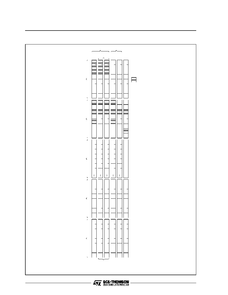
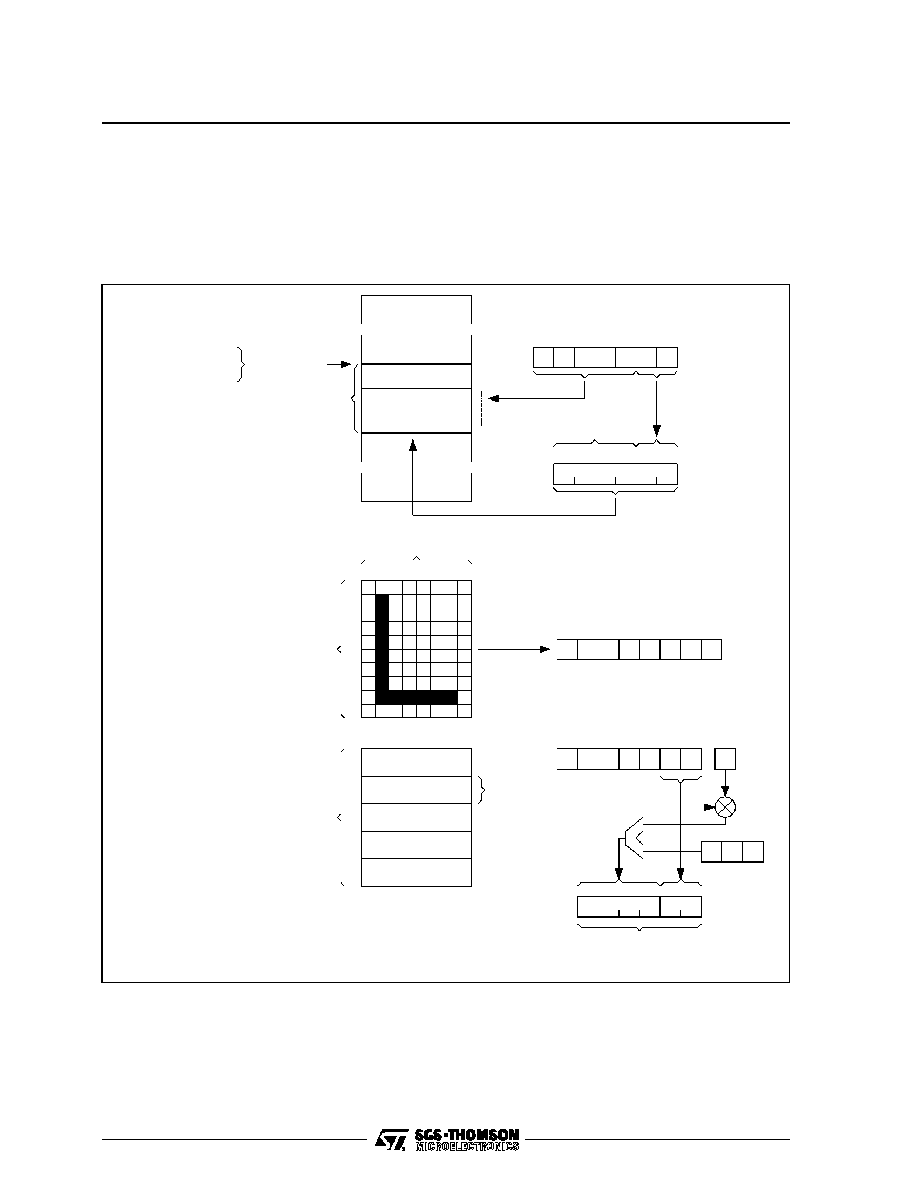
40 CHAR/ROW CHARACTER CODES
To display pages in 40 character per row format,
one out of three character code formats must be
selected :
- Fixed long (24 bits) code : all parallel attributes.
- Fixed short (16 bits) code : mix of parallel and
latched attributes.
- Variable (8/24 bits) code : all latched attributes.
Fixed short and variable codes are translated into
fixed long codes by EF9345 during the internal row
buffer loading process. The choice of the character
code format is obviously a display flexibility/mem-
ory size trade off, left up to the user.
Fixed Long Codes
This is the basic 40 char./row code. Each 8 pixels
x 10 lines character window, on the screen is
associated with a 3-byte code in memory, namely
the C, B and A bytes (Figure 13). A row on the
screen is associated with a 120 byte row buffer in
memory.
3-BYTE Code Structure
1. C7 is a don't care. Up to 128 characters may
be addressed in each set. Each user definable
set holds only 100 characters : C byte value
ranges from 00 to 03 and 20 to 7F (hexa).
2. B(4:7) give the type and set number of the
character.
3. All the bichrome characters have the same
attributes except that alphanumerics may be
underlined, semi-graphics cannot. Accentuated
alphanumerics allow orthogonal accentuating
of any one of the 32 lower case ROM characters
with any of 8 accents (see Figure 27).
4. Bichrome and quadrichrome characters use
two different coloring schemes.
For bichrome characters, character code byte A
defines a two color set by giving directly two color
values (Figure 14). The negative attribute ex-
changes the two values. Each bit of slice byte
selects one color value out of two.
The "A" byte in a quadrichrome character code
defines an ordered 4 color set (Figure 15). When
more than 4 bits are set, higher ranking bits are
ignored. When less than 4 bits are set, the color set
is completed with implicit "white" value. The slice
byte is shifted 2 bits at once at half the dot fre-
quency (
4MHz).
Each bit pair designates one color out of the 4 color
sets.
Quadrichrome characters allow displaying up to 4
different colors (instead of 2) in any 8 x 10 window
at the penalty of an halved horizontal resolution.
By programming the R attribute in byte B, one may
chose to keep the full vertical resolution (1 slice per
line) or to halve it (each slice is repeated twice). In
any case, it is possible to change the color set freely
from window to window and to mix freely all the
character types. So, fairly complex pictures may be
displayed at low memory cost.
Handling Long Codes
The KRF command allows an easy X, Y random
access or an X sequential access to/from the mi-
croprocessor from/to a memory row buffer (Fig-
ure 16).
7
6
5
4
3
2
1
0
L
m
H
i
C BYTE
B BYTE
Insert
Double height
Conceal
Double width
Type and set
N
F
B
1
G
1
R
1
B
0
G
0
R
0
A BYTE
Background color C
0
Flash (blink)
Foreground color C
1
Negative (reverse video)
Bichrome Code
7
6
5
4
3
2
1
0
k
R
i
Insert
Low resolution
Subset index
(low resolution only)
Set number
4 COLOR PALETTE
Quadrichrome Code
1
1
9345-16.EPS
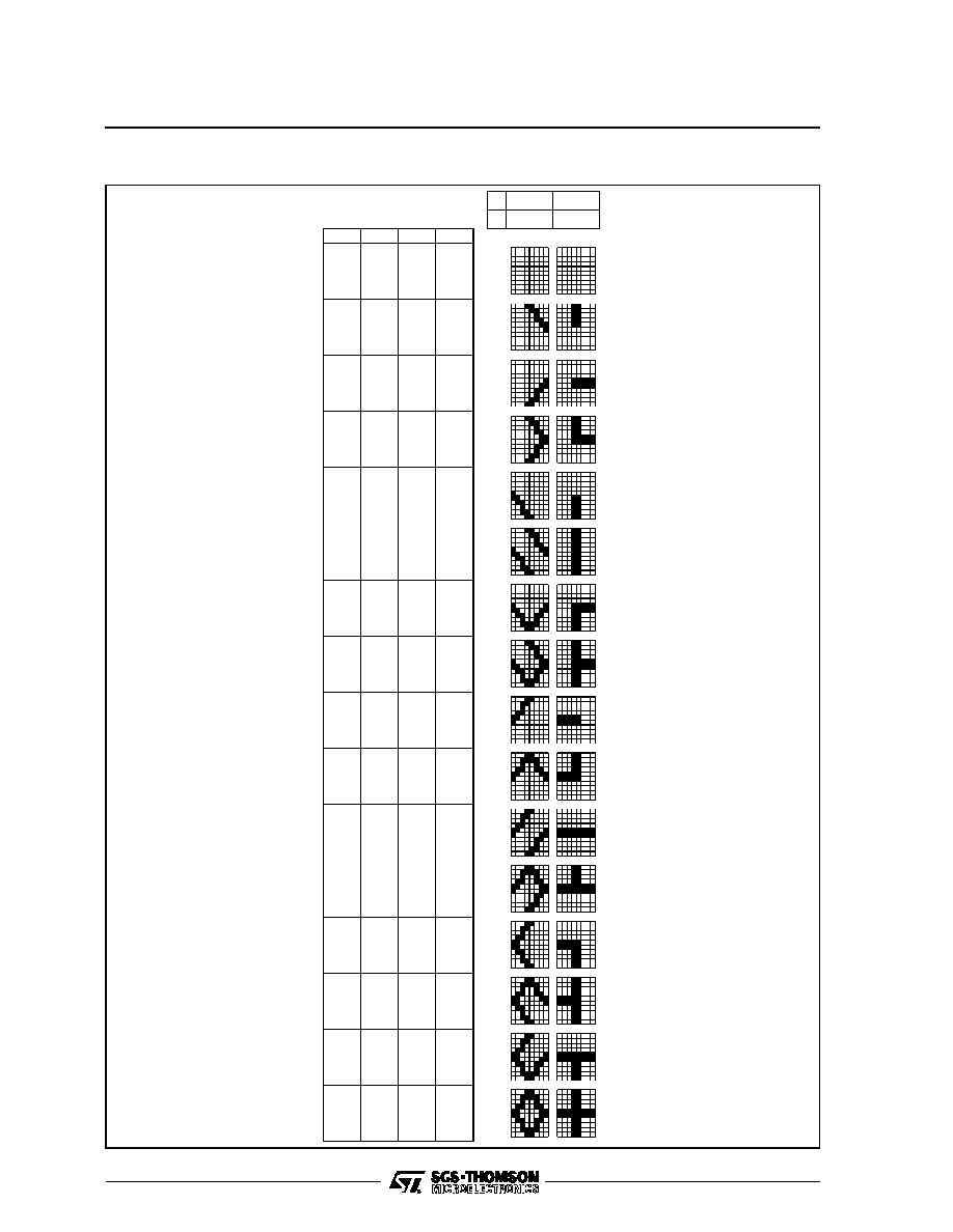
Figure 13 : 40 Char/Row Fixed Long Codes
EF9345
16/38
Figure 13 (Continued)
Type and Set
Code : B(4:7)
Number of Character
per Set
Set
Name
Set
Type
Cell
Location
7
6
5
4
C(0:6)
0
0
1
1
128 Standard MosaÔcs
32 Strokes
G
10
SEMI-GR
B
I
C
H
R
O
M
E
ON-CHIP
ROM
1
0
G
11
0
0
U
N
D
E
R
L
I
N
E
128 Alphanumerics
G
0
Accentuated Lower Case Alpha
ALPHA
1
0
G
20
1
G
21
1
0
0
100 Alpha UDS
G'
0
EXTERNAL
MEMORY
0
1
0
100 Semi-Graphic UDS
G'
10
SEMI-GR.
1
1
100 Semi-Graphic UDS
G'
11
1
X
X
8 Sets of 100
Quadrichrome Character
Q
0
to
Q
7
Quadrichrome
Note : Programming bit value : 1 = True ; 0 = False.
9345-08.TBL
7
6
5
4
3
2
1
0
N
F
B
1
G
1
R
1
B
0
G
0
R
0
CHARACTER
CODE A BYTE
7
6
5
4
3
2
1
0
3
3
N = 1
Exchanges values
3
3
C
1
C
0
Foreground
color
Background
color
3
R, G, B
Pixel color
MUX
0
1
0
1
0
0
1
0
Foreground
SHIFTED SLICE BYTE
(LSB first)
B
0
0
0
0
1
1
1
1
G
0
0
1
1
0
0
1
1
R
0
1
0
1
0
1
0
1
Color Value
Black
Red
Green
Yellow
Blue
Magenta
Cyan
White
9345-17.EPS
Figure 14 : Coloring with Bichrome Characters
EF9345
17/38
7
6
5
4
3
2
1
0
CHARACTER
CODE A BYTE
3
Black
3
C
1
(yellow)
MUX (1 out of 4)
0
1
0
1
1
0
1
0
ORDERED
COLOR VALUES
COLOR
SET
Red
Green
Yellow
Blue
Magenta
Cyan
White
_
C
0
_
C
1
C
2
_
C
3
_
7
6
5
4
3
2
1
0
0
1
C
1
C
0
C
2
C
3
3
3
3
Color set
2
SLICE BYTE SHIFTING :
2 bits at once at half the pixel frequency
9345-18.EPS
Figure 15 : Coloring with Quadrichrome Characters
R1
R2
R3
C
B
A
R4
R5
R6
R7
-
-
D, Y
B, X
KRF COMMAND
C
B
A
D district
number
B (even)
B + 1
B + 2
Y
X
0
39
9345-19.EPS
Figure 16 : Fixed Long Codes in Memory 120 Byte Row Buffer
EF9345
18/38
Variable Codes
In many cases, successive characters on screen
belong to the same character set and have the
same attributes. Variable codes achieve memory
saving by storing B and A bytes only when it is
required by exploiting the C7 bit.
C7 = 1 This is a long 3-byte code.
Character set and attribute values are
completely redefined by B and A bytes.
C7 = 0 This is a short 1-byte code.
Character set and attributes value are
identical to the previous code.
A further saving comes from the fact that an accen-
tuated alphabetic character is, more often than not,
followed by a not accentuated alphabetic character.
So, G
20
or G
21
sets are processed as one-shot
escape with return to G
0
. For normal operation,
variable codes should obey the following rules :
- The first character code of any row (X = 0) should
be long.
- A character code may be short when it has the
same attributes as the previous character code
and belongs to the same set.
However :
- Any code belonging to G
20
or G
21
must be long
and must be repeated if the character is double
width,
- A code belonging to G
0
following a G
20
or G
21
code may be short.
Handling the Variable Codes
During the display process, a row of variable code
should be laid in an 80/120 byte row buffer. The
first buffer holds the C bytes. The second buffer
holds the B, A file providing up to 20 long codes per
row (Figure 18). In the exceptional case when this
is not enough, the second buffer overflows in the
third one. Every code may then be long. Variable
codes can almost always achieve a memory saving
over long fixed codes and can never be worse.
The KRV command gives a very easy sequential
access to/from a row buffer from/to the microproc-
essor. This command automatically updates the C
byte and B, A file pointers (the last one when C7 is
set).
R1
R2
R3
-
-
-
R4
R5
R6
R7
ZW, YW
BF, XF
D, Y
B, X
EXP and CMP
COMMANDS
B
A
C
DW
BW (even)
BW + 1
B (even)
YW
X
0
39
BA
B + 1 = BF
D
Y
XF
VARIABLE
CODE
EXPANDED
CODE
9345-20.EPS
Figure 17 : Expansion/Compression Move
EF9345
19/38
Random access to a variable code is obviously not
as easy. The EXP, KRE and CMP commands are
designed to facilitate this task (figure 17).
The EXP command translates a full row of variable
codes into a row of expanded codes. Expanded
codes are generally not displayable by very similar
to the long codes.
KRE gives a random access to an expanded code
and makes it appear as a regular long code.
The CMP command translates a full row of ex-
panded code into a row of variabble codes and
minimizes the file size in the process.
These commands use a buffer pair as working
area.
Fixed Short Codes
These fixed 16 bits codes achieve memory saving
by another way. They may be easier to handlethan
variable codes. The penalty is in lesser display
capabilities :
- Accentuated character sets are no longer avail-
able : accentuated characters must be individu-
ally provided by the character generators.
- G'11 and quadrichrome sets cannot be reached.
- Some attributes are latched and can be changed
only while displaying a space (delimitor code).
The KRG command allows an easy access from/to
an 80-byte row buffer in memory to/from the micro-
processor (Figure 19). Figure 20 gives the fixed
short to fixed long translation process which occurs
for each row - while loading the internal row buffer
before display.
R1
R2
R3
C
B
A
R4
R5
R6
R7
-
BF, XF
D, Y
B, X
KRV COMMAND
BA
Overflow
buffer
D district
number
B (even)
XF :
file pointer
B + 2
Y
X
0
39
B + 1 = BF
9345-21.EPS
Figure 18 : Variable Codes in memory
R1
R2
R3
A*
B*
W
R4
R5
R6
R7
-
-
D, Y
B, X
KRG COMMAND
A*
B*
District
B (even)
B + 1
Y
X
0
39
9345-22.EPS
Figure 19 : Fixed Short Codes in Memory 80
EF9345
20/38
0
XXX
XXX
X
0
X
XXX
X
0
0
X
X
XXX
X
1
X
1
1
1
X
XXX
X
X
XXX
X
#00
#00
00
Ui
m
765
432
10
7
654
321
0
B*
A*
C
ALPHA
SEMI-
GRAPHIC
ALPHA
SEMI-
GRAPHIC
DEL
0
1
1
0
1
1
NL
H
F
F
F
F
F
C
1
NL
H
C
0
0
000
000
XX
XXX
X
X
XXX
XX
X
XXX
XX
X
XXX
XX
XXX
XX
0
1
#00
#00
C
1
C
0
N
0
0
N
0
1
F
F
F
F
F
0
0
001
0
0
0
0
0
0
00
0
0
0
H
H
i
L
L
m
m
m
m
m
m
U
U
U
BA
FIXED
LONG
CODE
FIXED
SHORT
CODE
G0
G10
G'0
G'10
Negative
space
R
O
M
M
E
M
O
R
Y
Latched
attribute
-
m
F
i
:
:
:
:
Don't
care
Conceal
Flash
Insert
N
U
X
DEL
:
:
:
:
Negative
Underline
Character
code
Deliminator
L
H
C
0
C
1
:
:
:
:
Double
width
Double
height
Background
color
Foreground
color
SET
Note
:
TRANSLATION
PROCESS
-
Field-to-field
:
a
character
code
or
an
attribute
value
(i.e
:
C
0
,
flashing)
is
directly
loaded
from
short
to
long
code.
The
translation
process
operates
through
3
elementary
operations
:
-
Field-to-constant
the
decoding
of
a
short
code
forces
the
value
of
the
equivalent
long
code
attribute.
For
example,
semigraphic
short
character
forces
normal
size
(H
=
0
,
L
=
0
)
attributes.
-
Latched
attributes
:
a
t
the
beginning
of
each
row,
these
attributes
are
reset
(no
underline,
not
concealed,
no
insert,
black
background).
Then,
they
keep
their
current
value
until
modified
by
either
a
field
to
constant
operation.
C
1
C
1
C
1
C
1
C
1
C
0
C
0
C
0
00
001
001
100
101
i
i
i
i
i
C
1
C
1
C
1
C
1
C
1
C
0
C
0
C
0
C
0
C
0
9345-23.EPS
Figure 20 : Fixed Short Code to Fixed Long Code Translation
EF9345
21/38
USED DEFINED CHARACTER GENERATOR IN MEMORY : DOR REGISTER
With 40 char / row, the elementary window dimen-
sions on the screen are 10 slices x 8 pixels. Thus,
a character cell holds 10 bytes in memory and 4
character cells are packed in one 40-byte buffer
(Figure 21). However, 5 bytes of a low resolution
quadrichrome cell are enough to fill up to window.
In this case, 8 character cells can be packed in one
40-byte buffer.
0 1 2 3 4 5 6 7
0
1
2
3
4
5
6
7
8
9
PIXELS
SLICE
NUMBER
(0 to 9)
NT
ONE SLICE
ONE BYTE
7
6
5
4
2
3
1
0
0
0
0
0
0
0
1
0
SLICES ARE SHIFTTED LSB FIRST
~
~
~
~
~
~
~
~
4 CHARACTER CELLS
0
39
ONE
1K BYTE
BLOCK
Z block address
Character set base address
and
Character set number
MEMORY
0
8
9
31
Y
X
C6 C5 C4 C3 C2 C1 C0
NT
5
4
2
3
1
0
A CHARACTER SET LAYS IN ONE BLOCK
(up to 100 characters per set)
Slice number
(0 to 9)
4
4
3
3
2
2
1
1
0
0
SLICE
NUMBER
(0 to 4)
NT
TWO SLICES
ONE BYTE (repeated)
C6 C5 C4 C3 C2 C1 C0
k
Character code C byte
(0 to 3 ; 32 to 127)
5
5
4
3
2
1
0
2
1
0
NT
NT*
X
+
NT* = 5k +NT
k = Subset index
A SPECIAL CASE : LOW RESOLUTION QUADRICHROME CELL (R = 1)
(up to 200 characters per set)
9345-24.EPS
Figure 21 : Packing UDS Cells in Memory
EF9345
22/38
The cells of one given character set should be layed
in one block.
Up to 100 character cells may be addressed in
each set (or 200 for low resolution quadrichrome
only). The location in memory, where to fetch the
sets in use, are declared by DOR register (Fig-
ure 22). For each type of set, it gives the MSB(s)
of the Z block address. EF9345 reads the Z LSB(s)
in the B byte of the (equivalent) long code. As usual,
the character code is read in the C byte. NT is
derived from the TV line rank in the row and the
double height status.
Loading User Defined Character Set
Before loading a character set into RAM, the user
must :
- Assign a name to the set :
∑
G'
0
, G'
10
or G'
11
for bichrome characters.
∑
From Q
0
to Q
7
for quadrichrome charac-
ters.
- Assign a character number to each character
belonging to this set, character numbers range
from 0 to 3 and 32 to 127.
∑
It is binary coded into 7 bits C(0:6) - C(0:6)
will be loaded later on into a C byte charac-
ter code in order to display the character.
- A pointer to a character slice in memory is then
manufactured from :
∑
The character number C(0:6)
∑
The slice number NT(0:3)
∑
The block number assigned to the set
Z(0:3)
Figure 23 shows how to proceed with the auxiliary
pointer and the OCT command.
Note : The main pointer may be also used. When
sequentially accessing slices of a given
character, auto incrementation is helpless.
7
6
5
4
3
2
1
0
Z
3
Z
3
Z
2
Z
1
Z
3
Z
2
Z
1
Z
0
DOR G'
1
DOR G'
0
DOR register
7
6
5
4
3
2
1
0
1
X
X
X
X
X
X
X
CHARACTER LONG
CODE B BYTE
~
~
~
~
~
~
~
~
~
~
~
~
~
~
~
~
~
~
~
~
DOR G'
0
(alpha UDS)
DOR G'
1
(semi-grap hic UDS)
DOR Q
(quadrichr ome)
Even block
Odd block
1 Kbyte
2 Kbytes
8 Kbytes
UDS Set
Z Address
#
B7 B6 B5
Z
3
Z
2
Z
1
Z
0
1
0
DOR
6
DOR
5
DOR
4
DOR
3
DOR
2
DOR
1
B4
G'
0
G'
11
Q0 - Q7
1
1
1
0
0
1
X
DOR
7
B4
B5
B3
MEMORY
G'
0
G'
10
G'
11
Q
0
Q
1
Q
7
DOR Q
DOR
0
9345-25.EPS
Figure 22 : UDS Fetch to Display
EF9345
23/38
Z
0
Z
1
Z
2
C6 C5 C4 C3 C2
C1 C0
NT
R4
R5
R6
R7
R1
R2
R3
SLICE
Y
X
Z
3
9345-26.EPS
Figure 23 : Accessing a Character Slice in Memory Using OCT Command with Auxiliary Pointer
On-Chip Character Generator
- G
0
set is common to 40 and 80 char./row modes
(Figure 24 and Figure 34).
- G
10
is the standard mosaÔc set for videotex (Fig-
ure 25).
- G
11
, G
20
and G
21
cannot be reached from the
16-bit short fixed codes (Figure 26 and Figure 27).
Displaying the Attributes
1.
For normal operation, a double height and/or
double width character must be repeated in
memory in two successive Y and/or X
positions. The user may otherwise freely mix
any character size.
2. The attributes are logically processed in the
following order :
- Underline or underline cursor : foreground
forced on the last slice (NT = 9).
- Flash : background periodically forced on the
whole window (0.5Hz). The phase depends on
the negative attribute.
- Conceal : background forced permanently on
the whole window. A concealed character
neither blinks nor is underlined.
- Negative : exchange the background and
foreground color values when set.
- Coloring.
- Complemented cursor mode.
- Insert : black color forced when required.
3. Basic pixel shift frequency : f
CLK
x 2/3 = 8MHz.
EF9345
24/38
0
0
0
0
C0
C1
C2
C3
0
0
0
1
0
0
0
1
0
0
1
1
0
0
0
1
0
0
1
1
0
1
0
1
1
0
1
1
0
0
0
1
0
0
1
1
0
1
1
1
0
0
1
1
0
1
1
0
1
1
0
1
1
1
1
0
C6
C5
C4
0
0
0
0
0
1
1
0
0
1
0
1
1
0
0
1
0
1
1
0
1
1
1
1
1
1
1
1
9345-27.EPS
Figure 24 : G
0
Alphanumeric Character Set in 40 Character/Row Mode
EF9345
25/38
0
0
0
0
C0
C1
C2
C3
0
0
0
1
0
0
0
1
0
0
1
1
0
0
0
1
0
0
1
1
0
1
0
1
1
0
1
1
0
0
0
1
0
0
1
1
0
1
1
1
0
0
1
1
0
1
1
0
1
1
0
1
1
1
1
0
1
1
1
1
C6
C5
C4
1
0
0
1
0
1
1
1
0
1
1
1
0
0
0
0
0
1
0
0
1
0
1
1
SEPARATED SEMI-GRAPHIC
MOSAIC SEMI-GRAPHIC
9345-28.EPS
Figure 25 : G
10
Semigraphic Character Set
EF9345
26/38
0
0
0
0
C0
C1
C2
C3
0
0
0
1
0
0
0
1
0
0
1
1
0
0
0
1
0
0
1
1
0
1
0
1
1
0
1
1
0
0
0
1
0
0
1
1
0
1
1
1
0
0
1
1
0
1
1
0
1
1
0
1
1
1
1
0
1
1
1
1
C5
C4
0
0
0
1
9345-29.EPS
Figure 26 : G
11
Stroke Set
EF9345
27/38
0
0
0
0
C0
C1
C2
C3
0
0
0
1
0
0
0
1
0
0
1
1
0
0
0
1
0
0
1
1
0
1
0
1
1
0
1
1
0
0
0
1
0
0
1
1
0
1
1
1
0
0
1
1
0
1
1
0
1
1
0
1
1
1
1
0
1
1
1
1
C4
0
1
C5
0
1
0
1
C6
0
1
0
1
B5
0
1
X
0
1
0
0
0
0
1
Byte C
0
1
0
0
X
X
X
X
Byte B
X
X
X
X
X
X
X
X
Byte A
7
6
5
4
3
2
1
0
Example :
X = bits defined by user
9345-30.EPS
Figure 27 : G
20
and G
21
Accentued Character Sets
EF9345
28/38
80 CHAR/ROW CHARACTER CODES
To display pages in 80 character per row format,
one of two character code formats must be se-
lected :
- Long (12 bits) code : 4 parallel attributes and large
on-chip 1024 semigraphic character set,
- Short (8 bits) code : no attribute, no semigraphic
set.
Both formats address the on-chip G0 set (128
characters 6 x 10). None allows UDS addressing.
Long Codes
Each 6 pixels x 10 lines character window on the
screen is associated with a 12-bit code in memory,
namely a C byte and an attribute nibble A (Fig-
ure 18). C7 bit designates the set.
- Alphanumeric set : C7 = 0
C(0:6) designates one out of 128 alphanumeric
characters in the G0 on-chip set. This set is
common to the 40 char/row format, with the 2 right
most columns truncated (see Figure 34).
A(0:3) gives 4 parallel attributes.
- MosaÔc set : C7 = 1
A(1:3) and C(0:6) address a dedicated mosaÔc
character. Each of these address bits controls the
foreground/background status of a 3 pixels x 2
lines sub-window : foreground when the bit is set.
A0 provides a color select attribute.
Short Codes
They are derived from the long code by giving a 0
implicit value to each bit of the A nibble : positive,
not underlined, not flashing.
Packing the Codes in Memory
Long codes are paired. A pair is packed in a 3-byte
word. Therefore, the 80 codes of a row fill a 120-
byte row buffer (Figure 29). The left most position
on the screen is even. Its corresponding C byte is
at the beginningof the first buffer. The next position
on the screen is odd. Its corresponding C byte is at
the beginning of the second buffer. Both nibbles
are packed in the third buffer. With short codes, the
same scheme yields 80-byte row buffers.
Access to the Codes in Memory
KRL command transfers 12 bits from/to the R1 and
R3 registers to/from memory. The read modify
write operation, necessary to write the A nibble in
memory, is automatically performed provided that
the A nibble is repeated in the R3 register (Fig-
ure 30). Dedicated auto-incrementationis also per-
formed when required.
KRC command does a similar job for the short
codes (Figure 31).
A very simple scheme allows the microprocessor
to transcode an horizontal screen location into a
pointer (Figure 32). The joint use of this scheme
with the dedicated command alleviates all the
packing/unpacking troubles.
7
6
5
4
3
2
1
0
0
X
C
X
X
X
X
X
X
3
N
2
F
1
U
0
D
A
7
6
5
4
3
2
1
0
1
X
C
X
X
X
X
X
X
3
X
2
X
1
X
0
D
A
ALPHANUMERIC CHAR CODE
N = Negative
F = Flash
U = Underline
D = Color set
128 ALPHANUMERICS
In G
0
set.
MOSAIC CHAR CODE
C0
C1
C2
C3
C4
C5
C6
A1
A2
A3
0
1
2
3
4
5
6
7
8
9
3 pels
3 pels
DEDICATED
MOSAIC SET
9345-31.EPS
Figure 28 : 80 Char/Row Character Code
EF9345
29/38
7
6
5
4
3
2
1
0
C
C
7
6
5
4
3
2
1
0
A
A
EVEN POSITION
ODD POSITION
PACKING 2 CODES
IN 3 BYTES
IN MEMORY
B (even)
B + 1
B + 2
9345-32.EPS
Figure 29 : 80 Char/Row Character Code Packing
7
6
5
4
3
2
1
0
R3
N
F
U
D
N
F
U
D
R1
R2
R3
C
-
A
R4
R5
R6
R7
-
-
D, Y
B, X
KRL Command
The A nibble should be respected
A
Y
D district
number
B
even
B + 1
odd
B + 2
Even
position
Odd
position
X
9345-33.EPS
Figure 30 : KRL Command : Sequential Access to Long Codes
EF9345
30/38

R1
R2
R3
C
-
-
R4
R5
R6
R7
-
-
D, Y
B, X
KRC Command
Y
D district
number
B (even)
B + 1 (odd)
X
9345-34.EPS
Figure 31 : KRC Command : Sequential Access to Short Codes
7
6
5
4
3
2
1
0
b1 X5 X4 X3 X2 X1 X0 b0
CHARACTER POSITION (0 to 79)
7
6
5
4
3
2
1
0
b1 X5 X4 X3 X2 X1 X0
b0
X = (0 to 39)
Block parity
Rotate right
9345-35.EPS
Figure 32 : Transcoding an Horizontal Screen Location into a R7 Pointer
7
6
5
4
3
2
1
0
I
1
B
1
G
1
R
1
I
0
B
0
G
0
R
0
C
1
C
0
B
M
G
M
R
M
X
X
D = 1
D = 0
C
M
DOR
MAT
Background
Color
Foreground
Color
D
N
i
0
0
1
1
0
1
0
1
i
0
i
0
i
1
i
1
C
M
C
0
C
M
C
1
C
0
C
M
C
1
C
M
The pixel shift frequency is f
CLK
(12MHz)
9345-36.EPS
Figure 33
Displaying the Attributes - DOR Register
Short code and mosaÔc characters are not flashing,
not underlined and "positive".
The attributesare processed in the following order :
- Underline or underlined cursor : foreground is
forced on the last slice (NT = 9).
- Flash : background is periodically (0.5Hz - 50%)
forced on all the window. The phase depends on
the negative attribute.
- Color select : a "positive" character is displayed
with a background color same as the margin
color. The foreground color is selected in DOR
register by the D attribute.
- Negative : when the character is negative, back-
ground and foreground colors are exchanged. In
complemented CURSOR position, these colors
are complemented.
- Insert : the D attribute selects one insert value in
DOR register. This attribute is then processed up
to the current insertion mode (see screen format
and attribute insert section.
EF9345
31/38
0
0
0
0
C0
C1
C2
C3
0
0
0
1
0
0
0
1
0
0
1
1
0
0
0
1
0
0
1
1
0
1
0
1
1
0
1
1
0
0
0
1
0
0
1
1
0
1
1
1
0
0
1
1
0
1
1
0
1
1
0
1
1
1
1
0
1
1
1
1
C6
C5
C4
0
0
0
0
0
1
1
0
0
1
0
1
1
0
0
1
0
1
1
0
1
1
1
1
0
0
0
0
0
0
0
0
C7
9345-37.EPS
Figure 34 : G
0
Alphanumeric Character Set in 80 Character/Row Mode
EF9345
32/38
MICROPROCESSOR ACCESS COMMANDS
A microprocessor bus cycle may transfer one byte
from/to the microprocessor to/from a directly ad-
dressable register. These registers provide an in-
direct access :
- To/from 5 on-chip indirect registers : ROR, DOR,
MAT, PAT and TGS.
- To/from the private memory.
Due to address/datamultiplexing, a bus cycle is a
2 phase process (see Timing diagram 1 or Timing
diagram 2).
Address Phase
The falling edge of AS latches to AD(0:7) bus state
and CS signal into the temporary A address register
(Figure 36).
- A(0:2) = i :
This register index designates one out of 8 direct
access registers Ri.
- A3 = XQR :
This is the execution request bit.
- A(4:7) = ASN :
This is the Auto-Selection Nibble
- A8 = LCS :
This is the latched value of CS input pin.
EF9345 is selected when the following condition is
met : ASN = 2(Hexa) and LCS = 0.
Therefore, EF9345 is mapped in the hexadecimal
microprocessor addressing space form XX20 to
XX2F, where XX is up to the user. Xhen EF9345 is
not selected, its AD bus pins float and no register
can be modified.
R1
R2
R3
R4
R5
R6
R7
DATA
REGISTERS
AUXILIARY
POINTER
MAIN
POINTER
7
6
5
4
3
2
1
0
7
6
5
4
3
2
1
0
7
6
5
4
3
2
1
0
CODE
PAR
D'
B'
X'
Y'
D
Y
B
X
0
0
COMMAND
REGISTER
(write only)
STATUS
REGISTER
(read only)
V sync status
LX
a
(X' = 39)
LX
m
(X = 39)
Alarm
Busy
R0
R1
7
9345-39.EPS
Figure 36 : Direct Access Registers
8
7
6
5
4
3
2
1
0
ADDRESS
REGISTER
(temporary)
Index register
Execution request (XOR)
Auto select nibble
(compared to 0010)
LCS (latched CS)
9345-38.EPS
Figure 35
EF9345
33/38
Data Phase - Registers
When EF9345 is selected and while AS input is low,
the Ri register is accessed.
R0 designates a write-only COMMAND register or
a read-only STATUS register.
R1 to R7 hold the arguments of a command. They
are read/write registers.
R1, R2, R3 are used to transfer the data.
R4, R5 hold the Auxiliary Pointer (AP).
R6, R7 hold the Main Pointer (MP).
(see memory organization ; pinter section for
pointer structure).
Command Register
This register holds a 4-bit command type and 4 bits
of orthogonal parameters (see command table).
Type
There are 4 groups of command :
The IND command which gives access to on-chip
resources,
The fixed format character code transfer com-
mands,
The variable character code handling commands,
The general purpose commands.
Parameters
R/W :
Direction
1 : to DATA registers (R1, R2, R3)
0 : from DATA registers.
r :
Internal resource index (see figure 27).
l :
Auto-incrementation
1 : with post auto-incrementation
0 : without auto-incrementation
p :
Pointer select
1 : auxiliary pointer
0 : main pointer
s, s :
Source, destination select
01 : source : MP ; destination : AP
10 : source : AP ; destination : MP
a, a :
Stop condition
01 : stop at end of buffer
10 : no stop.
Status Register
This is a read-only, direct access register.
S7 :
BUSY
BUSY is set at the beginningof any
command execution. It is reset at
completion.
S6 :
S5
S4 :
AI
LX
m
LXa
LXm or LXa is set when res-
pectively the main pointer or the
auxiliary pointer holds X = 39
before a possible incrementation.
The alarm bit S6 is set when LXm
or LXa is set and an incrementation
is performed after access.
S3 :
Gives the MSB value of R1.
S2 :
Gives the vertical synchronization
signal state.
This is maskable by the VRM
command.
S1 = S0 = 0
Not used.
S3 to S6 are reset at the beginning of any com-
mand.
The COMMAND TABLE shows every command
able to set, each of these status bits, after comple-
tion.
7
6
5
4
3
2
1
0
0
0
0
R/W
r
IND
COMMAND
R1
R2
R3
R4
R5
R6
R7
X
-
-
-
-
-
r
Register
0
1
2
3
4
5
6
7
ROM*
TGS
MAT
PAT
DOR
ROR
B6 C6 C5 C4 C3 C2
R6
...
B4 B5
3
2
1
0
C
1
C
0
NT
R7
1
* A slice in 400 only can be read from the internal
character generator.
The slice address must be initialized in R6, R7.
9345-40.EPS
Figure 37 : Indirect On-Chip Resource Access
EF9345
34/38
Notes on Command Execution
1. The execution of any command starts at the
trailing edge of DS when (and only when) :
- EF9345 has been selected,
- XQR has been set,
at the previous AS falling edge.
This scheme allows loading a command and its
argument in any order. For instance, a command,
once loaded, may be re-executed with new or partly
new arguments.
2. At power on, the busy state is undeterminated.
It is recommanded to load first a dummy
command with XQR = 1 before any effective
command.
3. While Busy is set, the current command is
under execution. Register access is then
restricted.
Register access with XQR = 0
- Read STATUS is effective.
- Write COMMAND or any other register access
are ineffective.
That is to say, the microprocessor reads undeter-
mined values and may not modify a register.
Register access with XQR = 1
- Read STATUS or write COMMAND are effective,
- Access to other registers is ineffective.
However, the previous command is aborted and
the new command execution launched (with an
initial state undetermined for registers and memory
locations handled by the aborted command).
4. Execution suspension
The execution of any command (except VRM,
VSM) is suspended during the last and first TV line
of an active row. This is because the memory bus
cannot be allocated for microprocessor access dur-
ing this 104
µ
s period.
This holds too for internal resource access because
on-chip data transfer uses internal data memory
bus.
IND Command (See Figure 37)
This command transfers one byte between R1 and
an internal resource. The r parameter designates
one on-chip indirect register.
Fixed Format Character Code Access :
KRF, KRG, KRL, KRC
Each of these commands is dedicated to transfer
one complete character code between DATA reg-
isters and memory. MP is exclusively used.
KRF transfers 24 bits.
KRG transfers 16 bits
KRL transfers 12 bits.
KRC transfers 8 bits.
Code packing, pointer and data structures are ex-
plained in the corresponding character code sec-
tion.
When auto-incrementation is enabled, MP is auto-
matically updated after access so as to point to the
next location. This location corresponds to the next
right position on screen. When last position (X = 39)
is accessed, LXm is set. When last position is
accessed with auto-incrementation, alarm is also
set. MP is then pointing back at the beginning of
the row : there is no automatic Y incrementation.
Variable Code Handling Commands :
KRV EXP, CMP, KRE
An overview on these commands is given in "han-
dling the variable codes" (40 char./row section).
KRV uses R5 to point the attribute file. LX
a
is set
when this file is full (the last attribute pair has been
accessed).
EXP and CMP use MP and R5 in the same way as
KRV. Furthermore, R4 points to a working double
buffer. Thse two commands process a whole row
buffer and stop either at the end of the row buffer
or when the file overflows. In the last case, the
alarm bit is set.
KRE uses MP to point to a buffer and R4 to point
to a working double buffer. R5 is unused. In other
respects, KRE is identical to KRL.
For these commands, R4(5:7) hold the LSB's block
dress of the working buffer W.
7
6
5
4
3
2
1
0
Z
0
Z
1
Z
2
R4
Y
YW
ZW
ZW
3
is given by bit 6 of R6
9345-41.EPS
Figure 38
EF9345
35/38
General Purpose Access to a Byte OCT
This command uses either MP or AP pointer.
When MP is in use, an overflow yields to a Y
incrementation.
Move Buffer Commands : MVB, MVD, MVT
These are memory to memory commands which
use R1 as working register.
MVB transfers a byte from source to destination,
post-increments the 2 pointers and iterates until the
stop condition is met. MVD and MVT are similar but
work respectively with 2 byte word and 3 byte word.
That is to say, MVB works on buffers, MVD on
double buffers and MVT on triple buffers. If the
parameter a = 1, the process stops when either
source or destination buffer end is reached. If the
parameter a = 0, the process never stops until
aborted. In this case, main pointer overflow yields
to a Y incrementation in MP. So, a whole block or
page may be initialized.
Miscellaneous Commands : INY, VRM and
VSM
INY command increments Y in MP.
VRM and VSM respectively reset and set a vertical
synchronization status mask. When the mask is
set, status bit S2 remains at 0. When the mask is
reset, status S2 follows the vertical sync. state : it
is reset for 2 TV lines per frame and stays at 1
during the remaining period. It becomes readable
by the microprocessor form the status register.
After power on, the mask state is undetermined.
Table 4 : Command
Type
Memo
Code
Parameter
Status
Arguments
Execution Time (1)
7
6
5
4
3
2
1
0
AI LX
m
LX
a
R17 R1 R2 R3 R4 R5 R6 R7
Write
Read
Indirect
IND
1
0
0
0
R/W
r
0
0
0
0
D
-
-
-
-
MP
2
3.5
40 Characters - 24 bits
KRF
0
0
0
0
R/W
0
0
I
X
X
0
0
C
B
A
-
-
MP
4
7.5
40 Characters - 16 bits
KRG
0
0
0
0
R/W
0
1
I
X
X
0
0
A* B* W
-
-
MP
5.5
7.5
80 Characters - 8 bits
KRC
0
1
0
0
R/W
0
0
I
X
X
0
0
C
-
-
-
-
MP
9
9.5
80 Characters - 12 bits
KRL
0
1
0
1
R/W
0
0
I
X
X
0
0
C
-
A
-
-
MP
12.5
11.5
40 Characters Variable
KRV
0
0
1
0
R/W
0
0
I
X
X
X
X
C
B
A
-
XF
MP
(2) 3 + 3 + j
3.5 +
6 * j
Expansion
EXP
0
1
1
0
0
0
0
0
X
0
X
0
C
B
A
PW XF
MP
(3) < 247
-
Compression
CMP
0
1
1
1
0
0
0
0
X
0
X
0
C
B
A
PW XF
MP
(3) < 402
-
Expanded Characters
KRE
0
0
0
1
R/W
0
0
I
X
X
0
0
C
B
A
PW
-
MP
4
7.5
Byte
OCT
0
0
1
1
R/W
p
0
I
X
X
X
0
D
-
-
AP
MP
4
4.5
Move Buffer
MVB
1
1
0
1
s
s
a
a
0
0
0
0
W
-
-
AP
MP
(2) 2 + 4. n
-
Move Double Buffer
MVD
1
1
1
0
s
s
a
a
0
0
0
0
W
-
-
AP
MP
(2) 2 + 8. n
-
Move Triple Buffer
MVT
1
1
1
1
s
s
a
a
0
0
0
0
W
-
-
AP
MP
(2) 2 + 12. n
-
Clear Page (4) - 24 Bits
CLF
0
0
0
0
0
1
0
1
X
X
0
0
C
B
A
-
-
MP
< 4700
(1 K code)
-
Clear Page (4) - 16 bits
CLG
0
0
0
0
0
1
1
1
X
X
0
0
A* B* W
-
-
MP
< 5800
(1 K code)
-
Vertical Sync Mask Set
VSM
1
0
0
1
1
0
0
1
0
0
0
0
-
-
-
-
-
-
-
1
-
Vertical Sync Mask Reset
VRM
1
0
0
1
0
1
0
1
-
-
-
-
-
-
-
-
-
-
-
1
-
Increment Y
INY
1
0
1
1
0
0
0
0
0
0
0
0
-
-
-
-
-
Y
-
2
-
No Operation
NOP
1
0
0
1
0
0
0
1
-
-
-
-
-
-
-
-
-
-
-
1
-
9345-09.TBL
P
:
Pointer select
1 : auxiliary pointer
0 : main pointer
s, s
:
Source, destination
01 : source = MP ;
destination = AP
10 : source = AP ;
destination = MP
a, a
:
Stop condition
01 : stop at end of buffer
10 : no stop
r
:
Indirect register number
-
:
Not affected
W
:
Used as working register
PW
(Z, YW)
:
Working buffer
X
:
Set or Reset
XF
:
X File
I
:
Pointer incrementation
D
:
Data
MP
:
Main pointer
AP
:
Auxiliary pointer
(1) Unit :
12 clock periods (
1
µ
s)
without possible suspension.
(2) n
:
total number of word
40 ;
j = 1 for long code,
j = 0 for short codes.
(3)
:
Worst case (20 long codes +
20 short codes).
(4)
:
These commands repeats KRF
or KRG with Y incrementation
when X overflows. When the
last position is reached in a
row. Y is incremented and the
process starts again on the
next row.
EF9345
36/38

EF9345
AD(0:7)
PORT C
AS
SC1
DS
E
R/W
SC2
CS
IOS
EF6801
9345-42.EPS
Figure 39 : Interface with EF6801
RAM
2K x 8
ET2128
A0-A7
ADM(0:7)
OE
ASM
WE
AM(8:10)
OE
CS
WE
EF9345
74LS
373
D0-D7
A8-A10
9345-43.EPS
Figure 40 : Minimum Application with 2K x 8
Memory
One page memory terminal in 16-bit fixed format or
24-bit compressed format.
RAM
8K x 8
A0-A7
ADM(0:7)
OE
ASM
WE
AM(8:12)
OE
CE
WE
EF9345
D0-D7
A8-A12
9345-44.EPS
Figure 41 : Typical Application with 8K x 8 Dy-
namic or Pseudoi-static RAM
Multipage terminal with possibility of multiple user
definable character sets.
DRAM
16K x 4
A0-A7
ADM(0:7)
G
ASM
W
OE
CAS
WE
EF9345
ADDRESS
MUX
2
x
74LS157
D0-D3
AM(8:13)
1/2
74LS74
D
Q
CK
1/2
74LS74
D
Q
CK
RAS
CLK
12MHz CLOCK
D4-D7
9345-45.EPS
Figure 42 : Maximum Application with 16K x 8
Memory
Multipage terminal with user definable character
sets and buffer areas.
EF9345
37/38
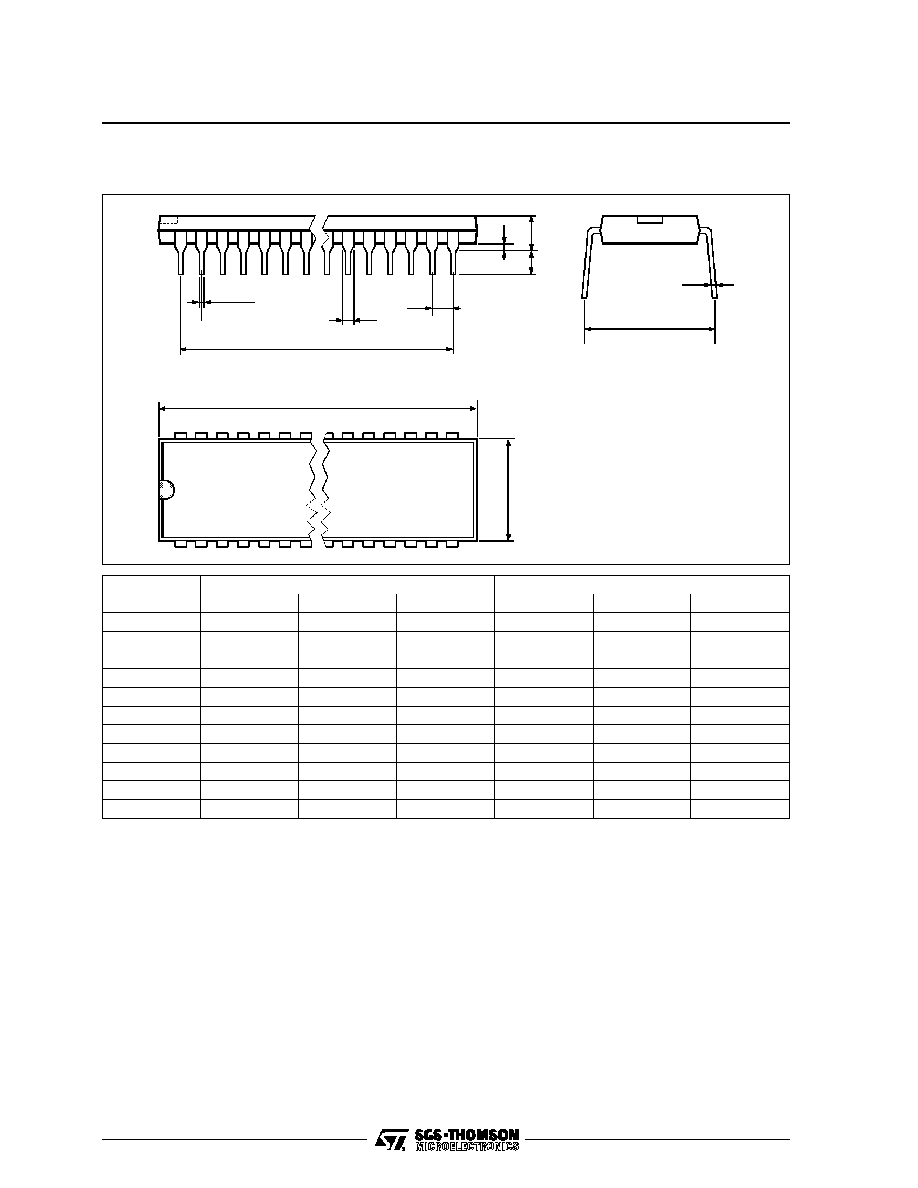
40
I
a1
L
b2
e
D
e3
F
b1
E
21
1
20
b
PM-DIP40.EPS
PACKAGE MECHANICAL DATA
40 PINS - PLASTIC DIP
Dimensions
Millimeters
Inches
Min.
Typ.
Max.
Min.
Typ.
Max.
a1
0.63
0.025
b
0.45
0.018
b1
0.23
0.31
0.009
0.012
b2
1.27
0.050
D
52.58
2.070
E
15.2
16.68
0.598
0.657
e
2.54
0.100
e3
48.26
1.900
F
14.1
0.555
i
4.445
0.175
L
3.3
0.130
DIP40.TBL
Information furnished is believed to be accurate and reliable. However, SGS-THOMSON Microelectronics assumes no responsibility
for the consequences of use of such information nor for any infringement of patents or other rights of third parties which may result
from its use. No licence is granted by implication or otherwise under any patent or patent rights of SGS-THOMSON Microelectronics.
Specifications mentioned in this publication are subject to change without noti ce. This publication supersedes and replaces all
information previously supplied. SGS-THOMSON Microelectronics products are not authorized for use as critical components in life
support devices or systems without express written approval of SGS-THOMSON Microelectronics.
©
1995 SGS-THOMSON Microelectronics - All Rights Reserved
Purchase of I
2
C Components of SGS-THOMSON Microelectronics, conveys a license under the Philips
I
2
C Patent. Rights to use these components in a I
2
C system, is granted provided that the system confo rms to
the I
2
C Standard Specifications as defined by Philips.
SGS-THOMSON Microelectronics GROUP OF COMPANIES
Australia - Brazil - China - France - Germany - Hong Kong - Italy - Japan - Korea - Malaysia - Malta - Morocco
The Netherlands - Singapore - Spain - Sweden - Switzerland - Taiwan - Thailand - United Kingdom - U.S.A.
EF9345
38/38