EMIF01-10018W5
Æ
September 1999 - Ed: 1
IEC 1000-4-2
15kV
(air discharge)
level 4
8 kV
(contact discharge)
MIL STD 883C - Methode 3015-6 Class 3
COMPLIES WITH THE FOLLOWING STANDARD:
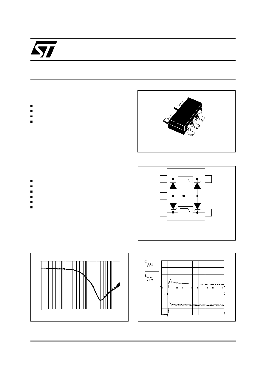
SOT323-5L
FUNCTIONAL DIAGRAM
I1
GND
I2
O1
O2
R
= 100
C
= 180pF
I/O
IN
Cost-effectiveness compared to discrete solution
EMI bi-directional low-pass filter
High efficiency in ESD suppression.
High flexibility in the design of high density boards
Very low PCB space consuming : 4.2 mm
2
typically
High reliability offered by monolithic integration
BENEFITS
EMI FILTER
INCLUDING ESD PROTECTION
Application Specific Discretes
A.S.D.
TM
Where EMI filtering in ESD sensitive equipment is required :
Computers and printers
Communication systems
Mobile phones
MCU Boards
MAIN APPLICATIONS
The EMIF01-10018W5 is a highly integrated array
designed to suppress EMI / RFI noise in all systems
subjected to electromagnetic interferences.
Additionally, this filter includes an ESD protection circuitry
which prevents the protected device from destruction when
subjected to ESD surges up to 15 kV.
DESCRIPTION
TM : ASD is trademark of STMicroelectronics.
Filtering behavior
ESD response to IEC1000-4-2 (16 kV air discharge)
Vin
Vout
1
10
100
1,000 2,000
-40
-30
-20
-10
0
f(MHz)
dB
1/10
Symbol
Parameter and test conditions
Value
Unit
V
PP
ESD discharge IEC1000-4-2, air discharge
ESD discharge IEC1000-4-2, contact discharge
ESD discharge MIL STD 883 Method 3015-6
16
9
25
kV
T
j
Junction temperature
150
∞C
T
op
Operating temperature range
-40 to + 85
∞C
T
stg
Storage temperature range
-55 to +150
∞C
T
L
Lead solder temperature (10 seconds duration)
260
∞C
ABSOLUTE MAXIMUM RATINGS (T
amb
= 25 ∞C)
Symbol
Test conditions
Min.
Typ.
Max.
Unit
V
BR
I
R
= 1 mA
6
7
8
V
I
RM
V
RM
= 3V
100
nA
R
I/O
80
100
120
R
d
I
pp
= 10 A, t
p
= 2.5
µ
s (see note 1)
1
C
IN
at 0V bias
180
pF
Note 1 : to calculate the ESD residual voltage, please refer to the paragraph "ESD PROTECTION" on pages 4 & 5
Symbol
Parameter
V
BR
Breakdown voltage
I
RM
Leakage current @ V
RM
V
RM
Stand-off voltage
V
CL
Clamping voltage
Rd
Dynamic resistance
I
PP
Peak pulse current
R
I/O
Series resistance between Input
and Output
C
IN
Input capacitance per line
ELECTRICAL CHARACTERISTICS (T
amb
= 25 ∞C)
V
I
V
RM
PP
I
RM
I
V
BR
R
I
V
CL
slope : 1 / R
d
EMIF01-10018W5
2/10
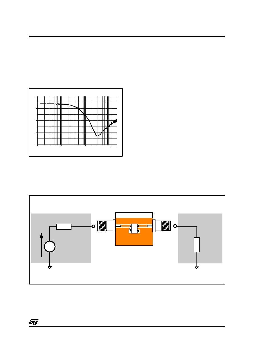
FREQUENCY BEHAVIOR
The EMIF01-10018W5 is firstly designed as an EMI/RFI filter. This low-pass filter is characterized by the following
parameters:
- Cut-off frequency
- Insertion loss
- High frequency rejection
Fig A1: EMIF01-10018W5 frequency response curve.
Fig. A2: Measurement conditions
1
10
100
1,000 2,000
-40
-30
-20
-10
0
f(MHz)
dB
TRACKING GENERATOR
Vg
50
TG OUT
SPECTRUM ANALYSER
50
RF IN
SMA
SMA
TEST BOARD
E
M
IF
0
1
TECHNICAL INFORMATION
Figure A1 gives these parameters, in particular the signal rejection at the GSM frequency is about
-24dB @ 900MHz
-20dB @ 1800MHz
EMIF01-10018W5
3/10
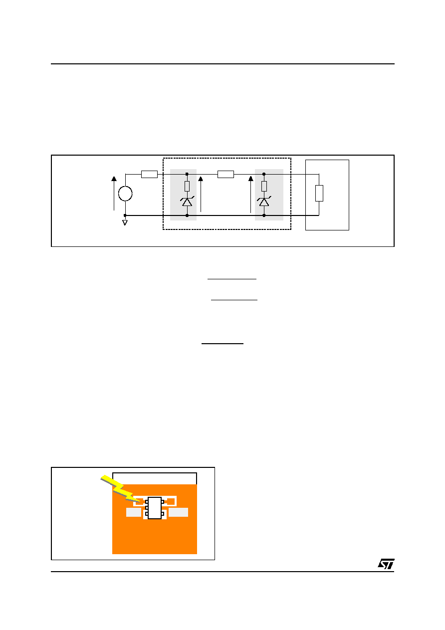
ESD PROTECTION
In addition to its filtering function, the EMIF01-10018W5 is particularly optimized to perform ESD protection.
ESD protection is based on the use of device which clamps at :
V
CL
= V
BR
+ R
d
.I
PP
This protection function is splitted in 2 stages. As shown in figure A3, the ESD strikes are clamped by the first stage S1 and
then its remaining overvoltage is applied to the second stage through the resistor R. Such a configuration makes the output
voltage very low at the Vout level.
Fig. A3: ESD clamping behavior.
ESD
Surge
Rload
Rg
Vg
Device to be protected
EMIF01-10018W5
Vin
Vout
R
S2
Rd
Vbr
S1
Rd
Vbr
Fig. A4: Measurement conditions
TEST BOARD
ESD
SURGE
EMIF01
16kV
Air
Discharge
Vin
Vout
To have a good approximation of the remaining voltages at both Vin and Vout stages, we provide the typical dynamical
resistance value Rd. By taking into account these following hypothesis : R>>Rd, R
G
>>Rd and Rload>>Rd, it gives these
formulas:
Vin
=
Rg.Vbr
+
Rd.Vg
Rg
Vout
=
R.Vbr
+
Rd.Vin
R
The results of the calculation done for an IEC 1000-4-2 Level 4 Contact Discharge surge (Vg=8kV, Rg=330
) and V
BR
=7V
(typ.) give:
Vin = 31.2 V
Vout = 7.3 V
This confirms the very low remaining voltage across the device to be protected. It is also important to note that in this
approximation the parasitic inductance effect was not taken into account. This could be few tenths of volts during few ns at
the Vin side. This parasitic effect is not present at the Vout side due the low current involved after the resistance R.
LATCH-UP PHENOMENA
The early ageing and destruction of IC's is often due to latch-up phenomena which mainly induced by dV/dt. Thanks to
its RC structure, the EMIF01-10018W5 provides a high immunity to latch-up by integration of fast edges. (Please see the
response of EMIF01-10018W5 to a 3 ns edge on Fig. A9)
The measurements done here after show very clearly (Fig. A5a & A5b) the high efficiency of the ESD protection :
- almost no influence of the parasitic inductances on Vout stage
- Vout clamping voltage very close to Vbr
EMIF01-10018W5
4/10
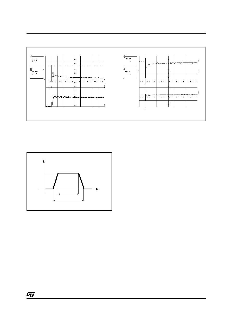
Fig. A6: Rd measurement current wave
Fig. A5: Remaining voltage at both stages S1 (Vin) and S2 (Vout) during ESD surge
Vin
Vout
Vin
Vout
a) Positive surge
b) Negative surge
2.5 µs
2 µs
t
t
I
I
PP
2.5 s duration measurement wave
µ
Please note that the EMIF01-10018W5 is not only acting for positive ESD surges but also for negative ones. For negatives
surges, it clamps close to ground voltage as shown in Fig. A5b.
NOTE: DYNAMIC RESISTANCE MEASUREMENT
As the value of the dynamic resistance remains stable for
a surge duration lower than 20
µ
s, the 2.5
µ
s rectangular
surge is well adapted. In addition both rise and fall times
are optimized to avoid any parasitic phenomenon during
the measurement of Rd.
EMIF01-10018W5
5/10