EMIF02-600FU7
Æ
September 1998 - Ed: 2A
IEC 1000-4-2
15kV
(air discharge)
8 kV
(contact discharge)
COMPLIESWITH THE FOLLOWING STANDARDS :
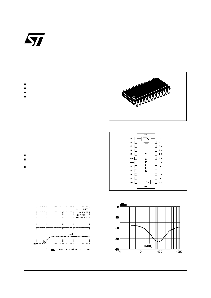
SSOP24
FUNCTIONAL DIAGRAM
.
.
.
10
C
E
L
L
S
.
.
.
10-bit EMI bi-directional low-pass-filter
Enhanced ESD protection for the protected device, op-
timized by the four point structure
High flexibility in the design of high density boards
BENEFITS
10-BIT WIDE EMI FILTER
INCUDING ESD PROTECTION
Application Specific Discretes
A.S.D.
TM
Where EMI filtering in ESD sensitive equipment is required :
Computers and printers
Communication systems
Mobile phones
MCU Boards
MAIN APPLICATIONS
The EMIF02-600FU7 is a highly integrated array designed
to suppress EMI / RFI noise in all systems subjected to
electromagnetic interferences.
Additionally, this filter includes an ESD protection circuitry
which prevents the protected device from destruction when
subjected
to
ESD
surges
up
to
15
kV.
The
EMIF02-600FU7 provides best efficiency when using
separated inputs and outputs, in the so-called 4-points
structure.
DESCRIPTION
TM : ASD is trademark of STMicroelectronics.
ESDresponseto IEC1000-4-2 (15 kVairdischarge)
Filtering response (with 50
line)
1/9
Symbol
Parameter and test conditions
Value
Unit
V
PP
ESD discharge IEC1000-4-2, air discharge
ESD discharge IEC1000-4-2, contact discharge
16
9
kV
T
j
Junction temperature
150
∞
C
T
op
Operatingtemperature range
-40 to + 85
∞
C
T
stg
Storage temperature range
-55 to +150
∞
C
T
L
Lead solder temperature (10 second duration)
260
∞
C
ABSOLUTE MAXIMUM RATINGS (T
amb
= 25
∞
C)
Symbol
Test conditions
Min.
Typ.
Max.
Unit
V
BR
I
R
= 1 mA
6
7
8
V
I
RM
V
RM
= 3V
1
µ
A
R
I/O
Serial resistance between Input and Output
480
600
720
R
d
I
pp
= 10 A, t
p
= 2.5
µ
s (see note 1)
0.55
Note 1 : to calculate the ESD residual voltage, please refer to the paragraph "ESD PROTECT ION" on pages 4 & 5
Symbol
Parameter
V
BR
Breakdown voltage
I
RM
Leakage current @ V
RM
V
RM
Stand-off voltage
V
CL
Clamping voltage
Rd
Dynamic impedance
I
PP
Peak pulse current
R
I/O
Serial resistance between Input
and Output
ELECTRICAL CHARACTERISTICS (T
amb
= 25
∞
C)
2.5
3.0
3.5
4.0
4.5
5.0
5.5
0.5
1.0
2.0
5.0
10.0
20.0
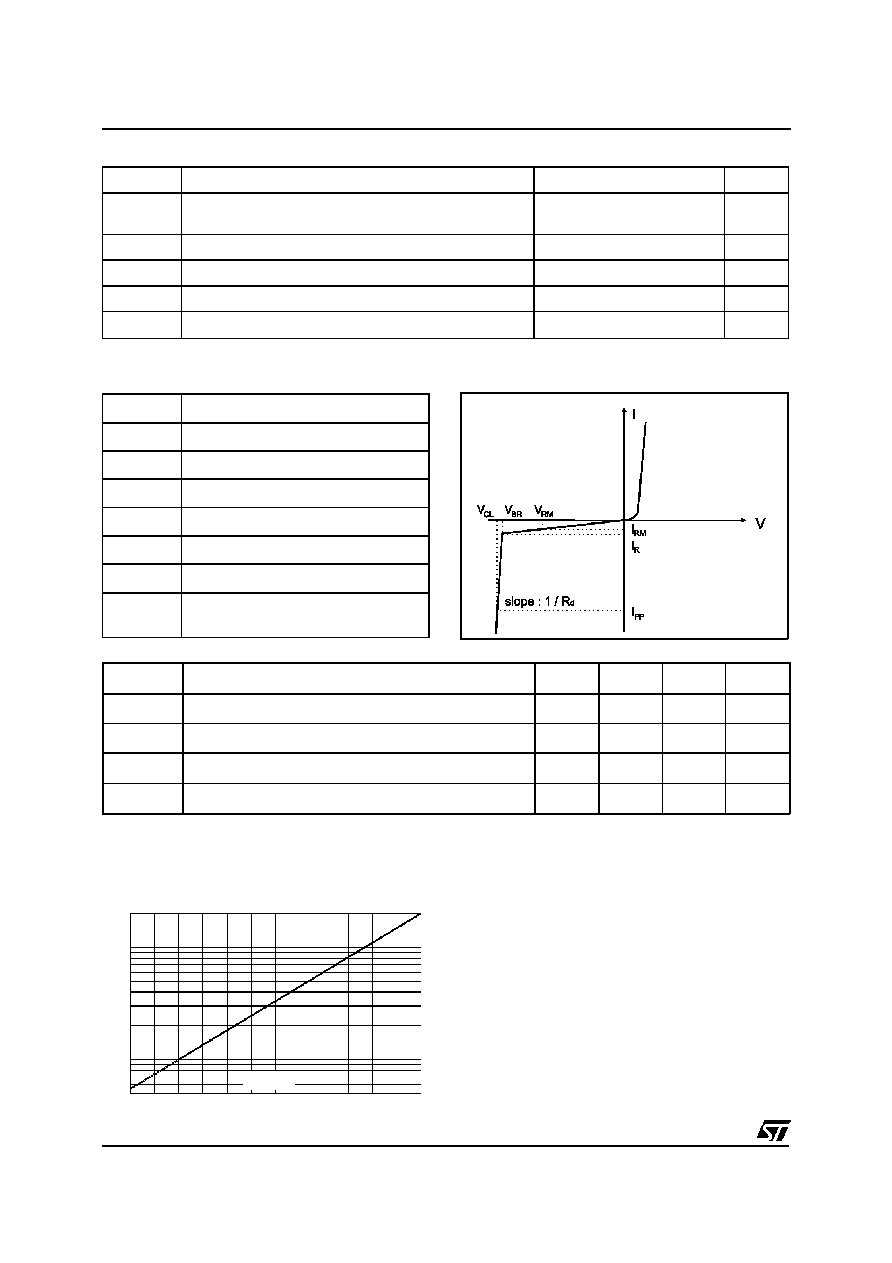
IR[VR] / IR[VR=3V]
VR (V)
Fig.1 : Relative variation of leakage current versus
reverse voltage(Typical values)
EMIF02-600FU7
2/9
TECHNICAL INFORMATION
FREQUENCY BEHAVIOR
The EMIF02-600FU7 is firstly designed as an EMI/RFI
filter. This low-pass filter is characterized by the following
parameters:
- Cut-off frequency
- Insertion loss
- High frequency rejection
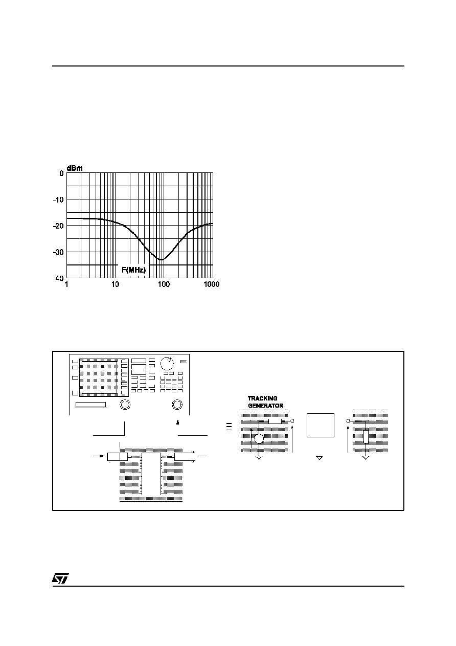
Figure A1 gives these parameters, in particular the signal rejection at the GSM frequency is about -20dBm at 900MHz,
while the attenuation for FM broadcast range (around 100MHz) is better than -32dBm
Fig A1 : EMIF02-600FU7frequencyresponse curve.
Fig A2 : Measurement conditions
TG OUTPUT
RF INPUT
EMIF02
TEST BOARD
EMIF02
SPECTRUM
ANALYSER
Vg
Vout
Vin
50
50
EMIF02-600FU7
3/9
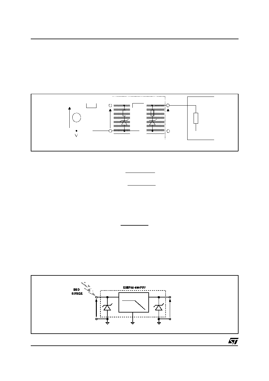
ESD PROTECTION
In addition to its filtering function, the EMIF02-600FU7 is particularly optimized to perform ESD protection.
ESD protection is based on voltage clamping which can be calculated by :
V
CL
= V
BR
+ R
d
.I
PP
This protection function is splitted in 2 stages. As shown in figure A3, the ESD strikes are clamped by the first stage S1 and
then its remaining overvoltage is applied to the second stage through the resistor R. Such a configuration makes the output
voltage V
out
very low.
To have a good approximation of the remaining voltages at both Vin and Vout stages, we provide the typical dynamical
resistance value Rd. By taking into account these following hypothesis : R>>Rd, R
G
>>Rd and Rload>>Rd, it gives these
formulas:
Vin
=
Rg.Vbr
+
Rd.Vg
Rg
Vout
=
R.Vbr
+
Rd.Vin
R
The results of the calculation done for V
G
=8kV, R
G
=330
(IEC1000-4-2 standard) and V
BR
=7V (typ.) give:
Vin = 20.33 V
Vout = 7.01 V
This confirms the very low remaining voltage across the device to be protected. It is also important to note that in this
approximation the parasitic inductance effect was not taken into account. This could be few tenths of volts during few ns at
the Vin side. This parasitic effect is not present at the Vout side due the low current involved after the resistance R.
The measurements shown here after illustrate very clearly (Fig. A5a) the high efficiency of the ESD protection :
- no influence of the parasitic inductances on Vout stage
- Vout clamping voltage very close to V
BR
Fig A3 : ESD clamping behavior
ESD
Surge
Vin
Vout
Rload
S1
S2
Rg
R
Rd
Rd
Vbr
Vbr
Vg
Device to be protected
EMIF02-600FU7
Fig A4 : Measurement conditions
GND
LOW-PASS FILTER
Vin
Vout
GND
GND
EMIF02-600FU7
4/9
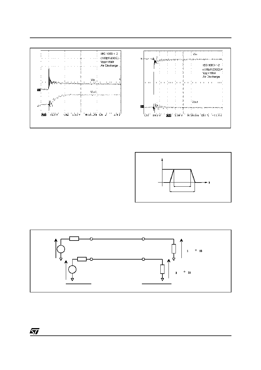
Please note that the EMIF02-600FU7 is not only acting for positive ESD surges but also for negative ones. For these kind
of disturbances it clamps close to ground voltage as shown in Fig. A5b.
NOTE: DYNAMIC RESISTANCE MEASUREMENT
As the value of the dynamic resistance remains stable for a
surge duration lower than 20
µ
s, the 2.5
µ
s rectangular surge
is well adapted. In addition both rise and fall times are
optimized to avoid any parasitic phenomenon during the
measurement of Rd.
CROSSTALK BEHAVIOR
1- Crosstalk phenomena
The crosstalk phenomena are due to the coupling between 2 lines. The coupling factor (
12
or
21
) increases when the
gap across lines decreases, particularly in silicon dice. In the example above the expected signal on load R
L2
is
2V
G2
, in
fact the real voltage at this point has got an extra value
21V
G1
. This part of the V
G1
signal represents the effect of the
crosstalk phenomenon of the line 1 on the line 2. This phenomenon has to be taken into account when the drivers impose
fast digital data or high frequency analog signals in the disturbing line. The perturbed line will be more affected if it works
with low voltage signal or high load impedance (few k
). The following chapters give the value of both digital and analog
crosstalk.
Fig A5 : Remaining voltage at both stages S1 (Vin) and S2 (Vout) during ESD surge
a) Positive surge
b) Negative surge
Fig A6 : Rd measurement current wave
2.5
µ
s
2
µ
s
t
t
I
I
PP
2.5
µ
s duration measurement w ave
Fig A7 : Crosstalk phenomena
line 1
line 2
V
G1
V
G2
R
G1
R
G2
R
L1
R
L2
DRIVERS
RECEIVERS
V
G1
V
G2
V
G2
V
G1
EMIF02-600FU7
5/9