
Æ
1/7
PRODUCT CHARACTERISTICS
ESD protection and EMI filtering for:
USB port
DESCRIPTION
The EMIF02-USB01F2 is a highly integrated array
designed to suppress EMI / RFI noise for USB
port filtering.
The EMIF02-USB01F2 flip-chip packaging means
the package size is equal to the die size.
Additionally, this filter includes an ESD protection
circuitry which prevents the protected device from
destruction when subjected to ESD surges up to
15 kV.
BENEFITS
2 lines low-pass-filter + 2 lines ESD protection
High efficiency in EMI filtering
Lead free package
Very low PCB space consuming: < 2.5 mm
2
Very thin package: 0.65 mm
High efficiency in ESD suppression
(IEC61000-4-2 level 4)
High reliability offered by monolithic integration
High reducing of parasitic elements through
integration & wafer level packaging.
COMPLIES WITH THE FOLLOWING STANDARDS:
IEC61000-4-2
Level 4
15kV (air discharge)
8kV (contact discharge)
EMIF02-USB01F2
2 LINES EMI FILTER
INCLUDING ESD PROTECTION
REV. 1
October 2004
IPADTM
Flip-Chip
(8 Bumps)
Figure 1: Pin Configuration (Ball side)
3
2
1
A
Pup
Vbus
DZ
GND
D+
in
D-
in
D+
out
D-
out
B
C
D
E
Table 1: Order Code
Part Number
Marking
EMIF02-USB01F2
FF
TM: IPAD is a trademark of STMicroelectronics.
Figure 2: Configuration
GND
Vbus
DZ
1.3K
D+ out
D- out
D- in
D+ in
Pup
33
33

EMIF02-USB01F2
2/7
Table 2: Absolute Ratings (T
amb
= 25∞C)
Table 3: Electrical Characteristics (T
amb
= 25∞C)
Symbol
Parameter and test conditions
Value
Unit
T
j
Junction temperature
125
∞C
T
op
Operating temperature range
- 40 to + 85
∞C
T
stg
Storage temperature range
- 55 to + 150
∞C
Symbol
Parameter
V
BR
Breakdown voltage
I
RM
Leakage current @ V
RM
V
RM
Stand-off voltage
V
CL
Clamping voltage
Rd
Dynamic impedance
I
PP
Peak pulse current
R
I/O
Series resistance between Input &
Output
C
line
Input capacitance per line
Symbol
Test conditions
Min.
Typ.
Max.
Unit
V
BR
I
R
= 1 mA
6
V
I
RM
V
RM
= 3V
0.5
µA
C
line
@ 0V
40
45
pF
R
1,
R
2
Tolerance ± 5%
33
R
3
Tolerance ± 5%
1.30
k
slope: 1/Rd

EMIF02-USB01F2
3/7
Figure 3: S21 (dB) attenuation measurement
Figure 4: Analog crosstalk measurements
Figure 5: ESD response to IEC61000-4-2 (+15kV
air discharge) on one input V(in) and on one
output (Vout)
Figure 6: ESD response to IEC61000-4-2 (-15kV
air discharge) on one input V(in) and on one
output (Vout)
Figure 7: Capacitance versus reverse applied
voltage (typical)
1.0M
3.0M
10.0M
30.0M
100.0M
300.0M
1.0G
3.0G
-50.00
-45.00
-40.00
-35.00
-30.00
-25.00
-20.00
-15.00
-10.00
-5.00
0.00
EMIF02-USB01: filtering response of lines C1/C3 and E1/E3
dB
Frequency/Hz
0.00
C1_C3
E1_E3
1.0M
3.0M
10.0M
30.0M
100.0M
300.0M
1.0G
3.0G
-100.0
-90.00
-80.00
-70.00
-60.00
-50.00
-40.00
-30.00
-20.00
-10.00
0.00
dB
f/Hz
100ns/d
Vin : 10V/d
Vout : 10V/d
100ns/d
Vin : 5V/d
Vout : 5V/d
10
15
20
25
30
35
40
0
0.5
1
1.5
2
2.5
3
3.5
4
4.5
5
VR(V)
C(pF)

EMIF02-USB01F2
4/7
Figure 8: Aplac model (resistors, diodes and bumps and ground connections)
Figure 9: Aplac model parameters
0.15nH
bulk
rsub_1k3
Csub
Csub
bulk
R_33R
cap_33R
C3
rsub_33R
cap_33R
Csub
Csub
E1
0.23nH
C1
A3
R_1k3
Csub
Csub
3.8nH
rsub_1k3
rsub_33R
0.3nH
bulk
R_33R
cap_33R
E3
rsub_33R
cap_33R
Csub
Csub
0.7nH
rsub_33R
D2
bulk
A1, A3, B2, C1, C3, E1, E3
0.15nH
Lgnd_D
Rsub_D
D02_usb
D02_Nw
D02_usb
D2
Lbump
Rbump
Lhole
Rhole
caphole
bulk
Cbump Rsubump
I/O
bulk
100m
D2
R_33R 33.9
cap_33R 1.2pF
R_1k3 1.3k
Cz29pF
Rsub_D 100
Csub0.3pF
Rsub_33R 15
Rsub_1k3 50
lhole10pH
Rhole400m
Caphole0.4pF
Lgnd_D 150pH
Lbump50pH
Rbump50m
Cbump1.5pF
Rsubump150
R_33R 33.9
cap_33R 1.2pF
R_1k3 1.3k
Model D02_usb
BV=16
IBV=1m
CJO=Cz
M=0.3333
RS=2
VJ=0.6
TT=100n
Model D02_Nw
BV=100
IBV=1m
CJO=6.8p
M=0.3333
RS=2
VJ=0.6
TT=100n
EMIF02-USB01F2
5/7
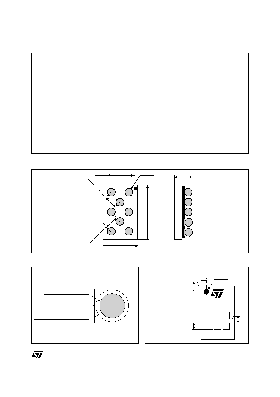
Figure 10: Ordering Information Scheme
Figure 11: FLIP-CHIP Package Mechanical Data
Figure 12: Foot print recommendations
Figure 13: Marking
EMIF yy - xxx zz Fx
EMI Filter
Number of lines
Information
Package
x = resistance value (Ohms)
z = capacitance value / 10(pF)
or
3 letters = application
2 digits = version
F = Flip-Chip
x
= 1: 500µm, Bump = 315µm
= 2: Leadfree Pitch = 500µm, Bump = 315µm
= 3: Leadfree Pitch = 400µm, Bump = 250µm
495µm
±
50
495µm
± 50
1.27mm ± 50µm
1.97mm ± 50µm
315 ± 50
700 ± 50
650µm ± 65
Copper pad Diameter :
250µm recommended , 300µm max
Solder stencil opening : 330µm
Solder mask opening recommendation :
340µm min for 315µm copper pad diameter
365
240
220
E
All dimensions in µm
Dot, ST logo
xx = marking
yww = datecode
(y = year
ww = week)
z = packaging location
365
40
x x z
y w w