July 2006
Rev 1
1/9
EMIF06-1005M12
6 line low capacitance EMI filter and ESD protection
IPADTM in Micro QFN package
Main product characteristics
Where EMI filtering in ESD sensitive equipment is
required:
LCD and CAMERA for Mobile phones
Computers and printers
Communication systems
MCU Boards
Description
The EMIF06-1005M12 is a 6 line highly integrated
device designed to suppress EMI/RFI noise in all
systems exposed to electromagnetic interference.
This filter includes ESD protection circuitry, which
prevents damage to the application when
subjected to ESD surges up to 15 kV on the input
pins.
Benefits
EMI symmetrical (I/O) low-pass filter
High efficiency in EMI filtering: -34 dB at
frequencies from 900 MHz to 1.8 GHz
Very low PCB space consuming:
2.5 mm x 1.5 mm
Very thin package: 0.6 mm max
High efficiency in ESD suppression on inputs
pins (IEC 61000-4-2 level 4).
High reliability offered by monolithic integration
High reduction of parasitic elements through
integration and wafer level packaging.
Lead free package
Complies with following standards:
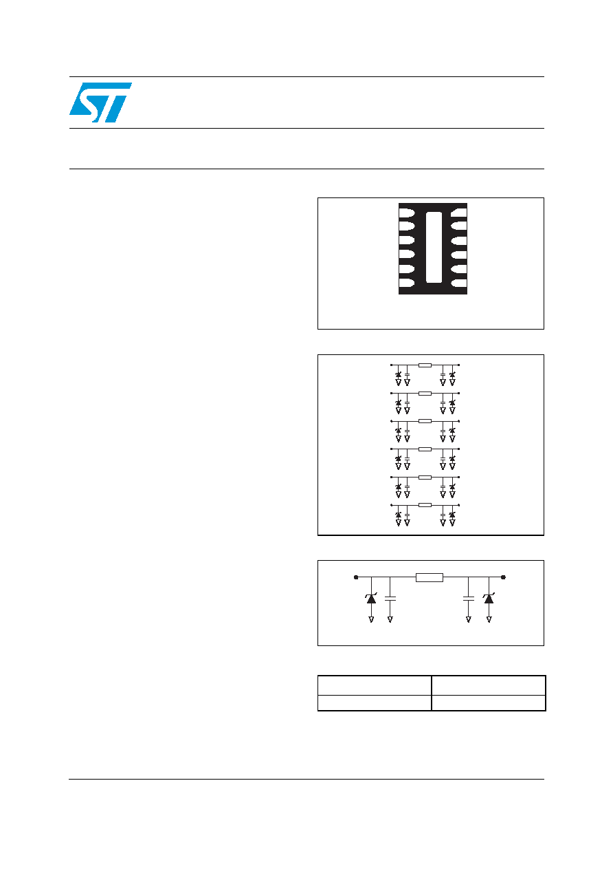
Pin configuration (top view)
Basic cell configuration
Order code
TM: IPAD is a trademark of STMicroelectronics
IEC 61000-4-2
level 4 input and output pins
15kV (air discharge)
8kV (contact discharge)
MIL STD 883E - Method 3015-6 Class 3 (all pins)
Part number
Marking
EMIF06-1005M12
F
1
2
3
4
GND
5
6
12
11
10
9
8
7
1
2
3
4
GND
5
6
12
11
10
9
8
7
Micro QFN 2.5 mm x 1.5 mm
(bottom view)
1 Input
Output 12
Output 11
Output 10
Output 9
Output 8
Output 7
2 Input
3 Input
4 Input
5 Input
6 Input
Typical line capacitance = 45 pF @ 0 V
100
Input
Output
www.st.com
Characteristics
EMIF06-1005M12
2/9
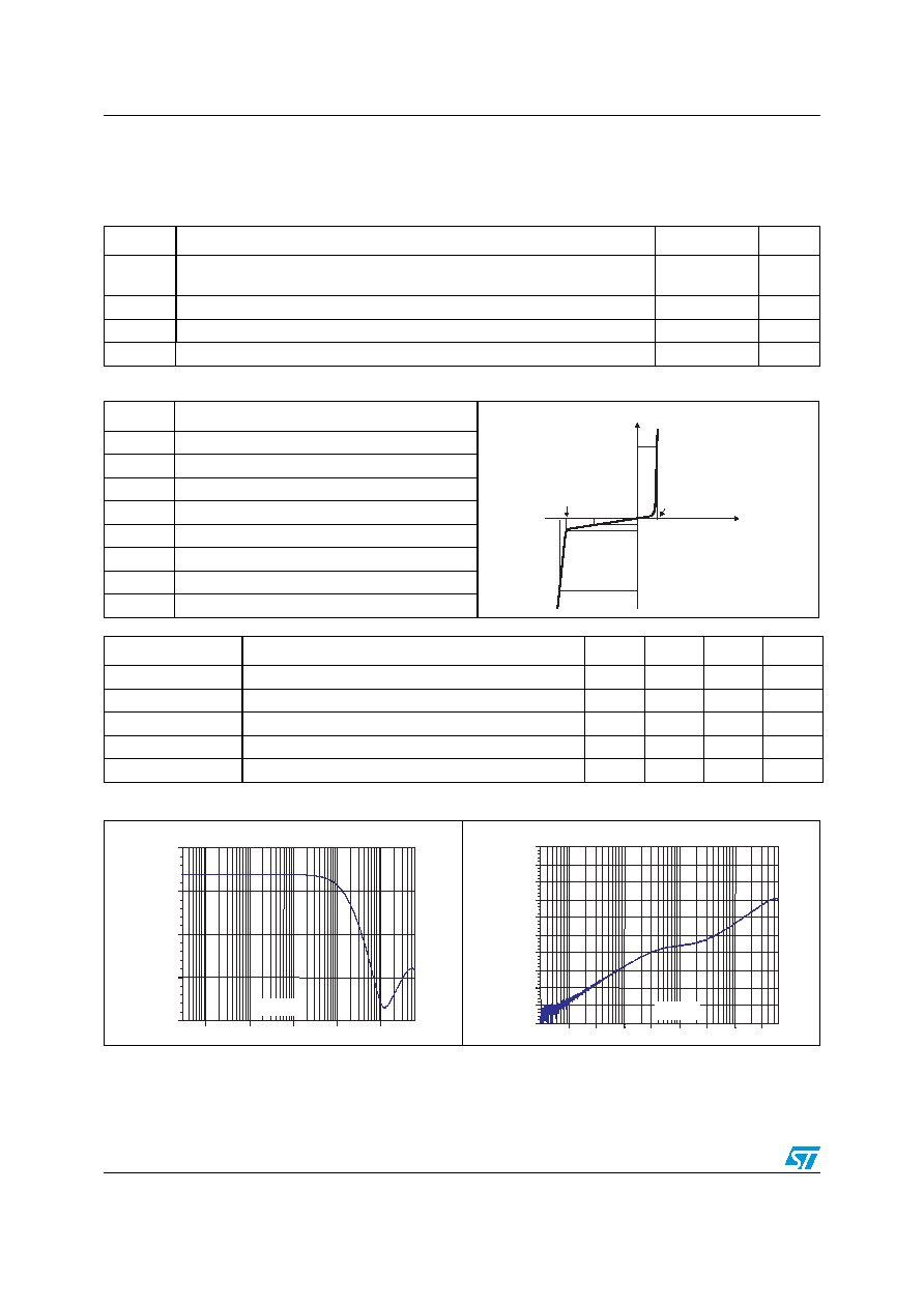
1 Characteristics
Table 1.
Absolute ratings (limiting values at T
amb
= 25° C unless otherwise specified)
Symbol
Parameter
Value
Unit
V
PP
ESD discharge IEC 61000-4-2 air discharge on input pins
ESD discharge IEC 61000-4-2 contact discharge on input pins
15
8
kV
T
j
Junction temperature
125
°C
T
op
Operating temperature range
-40 to + 85
°C
T
stg
Storage temperature range
-55 to +150
°C
Table 2.
Electrical characteristics (T
amb
= 25° C)
Symbol
Parameter
V
BR
Breakdown voltage
I
RM
Leakage current @ V
RM
V
RM
Stand-off voltage
V
CL
Clamping voltage
R
d
Dynamic resistance
I
PP
Peak pulse current
R
I/O
Series resistance between Input & Output
C
line
Input capacitance per line
V
BR
I
PP
V
RM
V
F
I
F
I
I
RM
I
R
V
V
CL
Symbol
Test conditions
Min.
Typ.
Max.
Unit
V
BR
I
R
= 1 mA
6
8
10
V
V
F
I = 10 mA
0.5
1.0
1.5
I
RM
V
RM
= 3 V per line
200
nA
R
I/O
Tolerance ± 10%
90
100
110
C
line
V
R
= 0 V
38
45
52
pF
Figure 1.
S21(dB) attenuation measurement
Figure 2.
Analog cross talk measurements
dB
100.0k
1.0M
10.0M
100.0M
1.0G
- 40.00
- 30.00
- 20.00
- 10.00
0.00
F (Hz)
1.0M
3.0M
10.0M 30.0M 100.0M 300.0M
1.0G
3.0G
- 100.00
- 90.00
- 80.00
- 70.00
- 60.00
- 50.00
- 40.00
- 30.00
- 20.00
- 10.00
0.00
F (Hz)
dB
EMIF06-1005M12
Ordering information scheme
3/9
2
Ordering information scheme
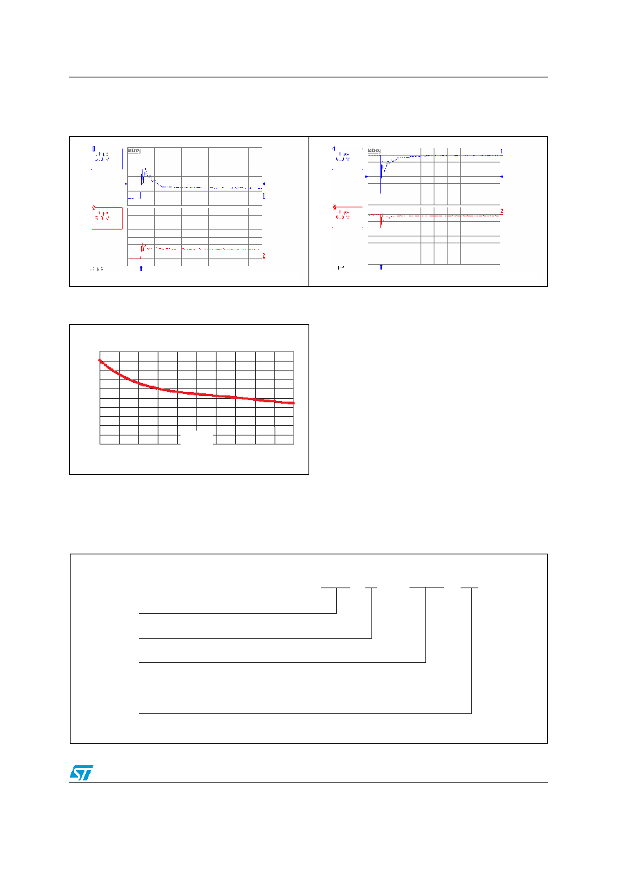
Figure 3.
ESD response to IEC 61000-4-2
(+15 kV air discharge) on one input
(V
in
) and on one output (V
out
)
Figure 4.
ESD response to IEC 61000-4-2
(- 15 kV air discharge) on one input
(V
in
) and on one output (V
out
)
Figure 5.
Line capacitance versus reverse
voltage applied (typical value)
0.00
5.00
10.00
15.00
20.00
25.00
30.00
35.00
40.00
45.00
50.00
0
1
2
3
4
5
V
LINE
(V)
C
LINE
(pF)
EMIF yy - xxx z Mx
EMI Filter
Number of lines
Information
Package
x = resistance value (Ohms)
z = capacitance value / 10(pF)
Mx = Micro QFN x leads
EMIF06-1005M12
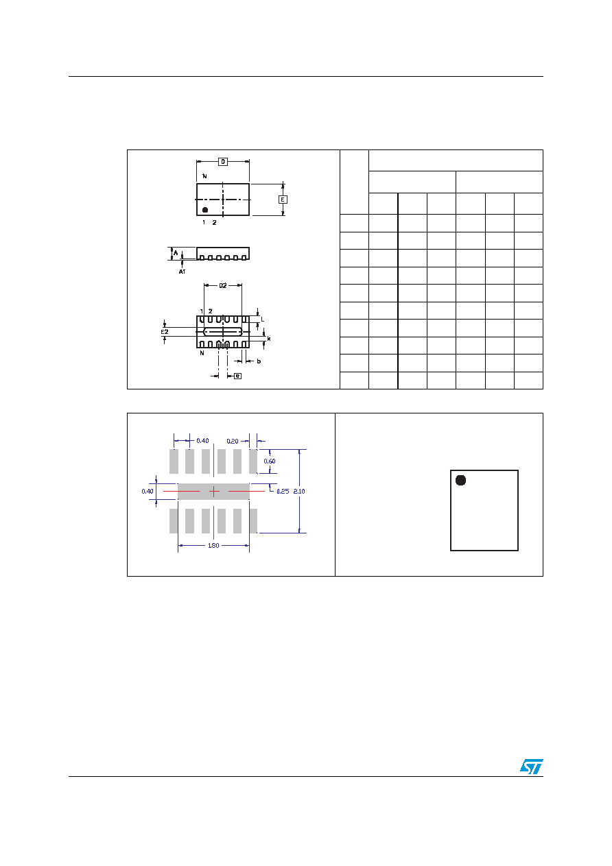
Package information
5/9
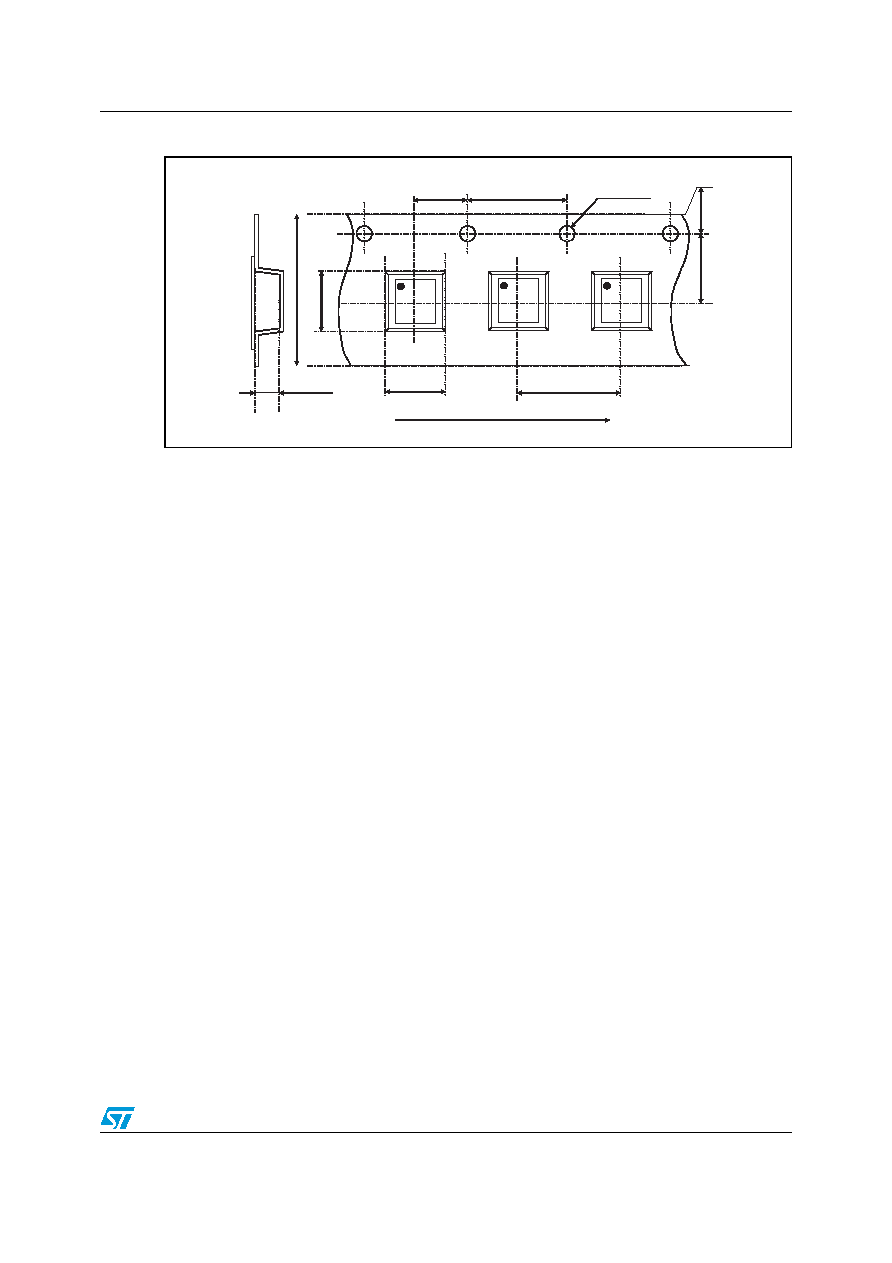
Figure 8.
Tape and reel specification
In order to meet environmental requirements, ST offers these devices in ECOPACK®
packages. These packages have a lead-free second level interconnect. The category of
second level interconnect is marked on the package and on the inner box label, in
compliance with JEDEC Standard JESD97. The maximum ratings related to soldering
conditions are also marked on the inner box label. ECOPACK is an ST trademark.
ECOPACK specifications are available at: www.st.com.
4.00+/-0.1
1.
75
+
/
-
0
.
1
4.00
f 1.5 +/- 0.1
3.
5
+
/
-
0.
05
User direction of unreeling
8.
1
+
/
-
0.
1
0.75
1.70
2.
70
2.0+/-0.05
XY
ww
XY
ww
XY
ww
4.00+/-0.1
1.
75
+
/
-
0
.
1
4.00
f 1.5 +/- 0.1
3.
5
+
/
-
0.
05
User direction of unreeling
8.
1
+
/
-
0.
1
0.75
1.70
2.
70
2.0+/-0.05
XY
ww
XY
ww
XY
ww
XY
ww
XY
ww
XY
ww