Äîêóìåíòàöèÿ è îïèñàíèÿ www.docs.chipfind.ru
®
1/9
ESDA14V2-4BF1
QUAD BIDIRECTIONAL TRANSILTM ARRAY
FOR ESD PROTECTION
REV. 2
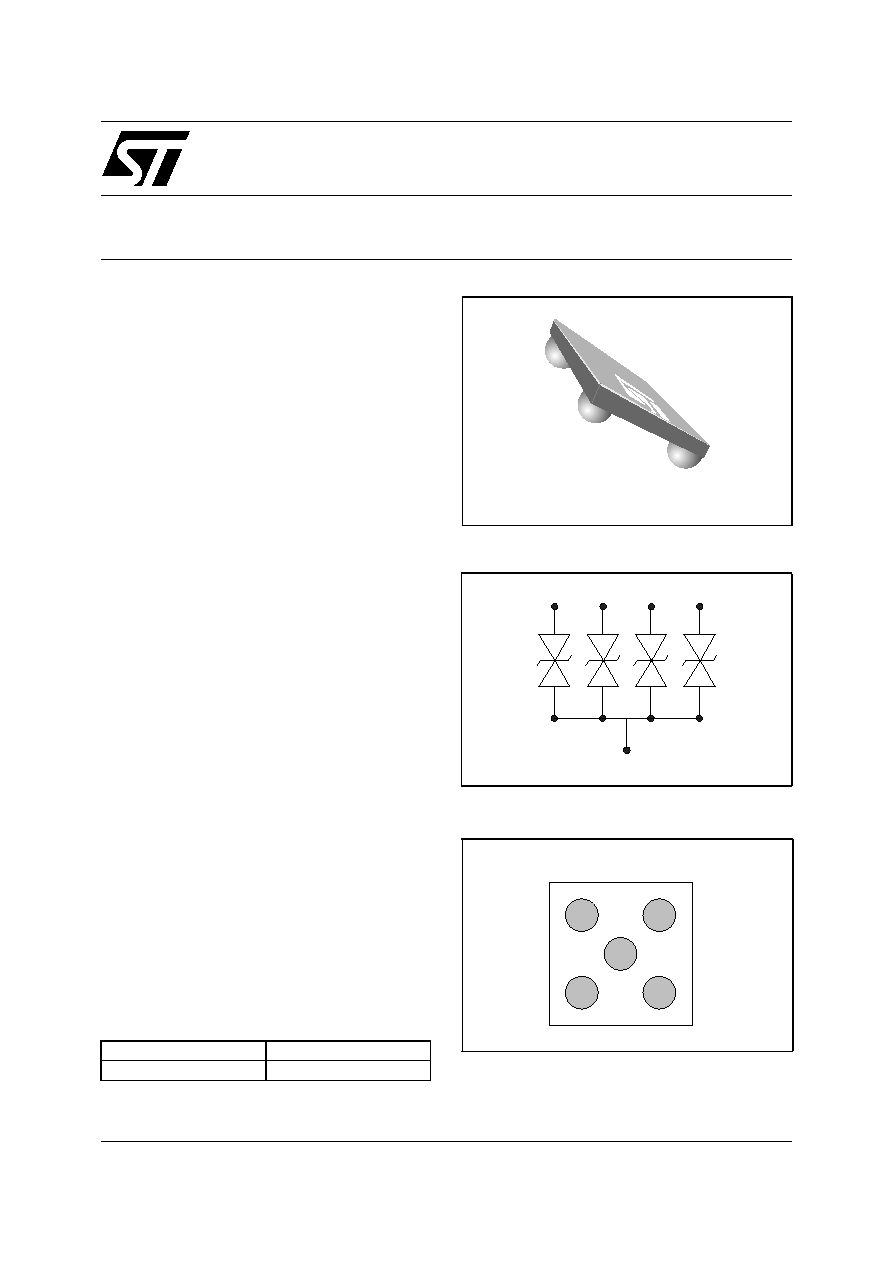
Flip-Chip
(5 bumps)
May 2004
APPLICATION
Where transient overvoltage protection in ESD
sensitive equipment is required, such as :
Computers
Printers
Communication systems and cellular phones
Video equipment
This device is particularly adapted to the
protection of symmetrical signals.
DESCRIPTION
The ESDA14V2-4BF1 is a monolithic array
designed to protect up to 4 lines in a bidirectional
way against ESD transients.
The device is ideal for situations where board
space saving is requested.
FEATURES
4 Bidirectional TransilTM functions
ESD Protection: IEC61000-4-2 level 4
Stand off voltage: 12 V MIN.
Low leakage current < 1 µA
50W Peak pulse power (8/20µs)
BENEFITS
High ESD protection level
High integration
Suitable for high density boards
COMPLIES WITH THE FOLLOWING STANDARDS:
- IEC61000-4-2: 15kV
(air discharge)
8kV
(contact discharge)
- MIL STD 883E- Method 3015-7: class3
25kV
(human body model)
Order Codes
Part Number
Marking
ESDA14V2-4BF1
EA
ASDTM
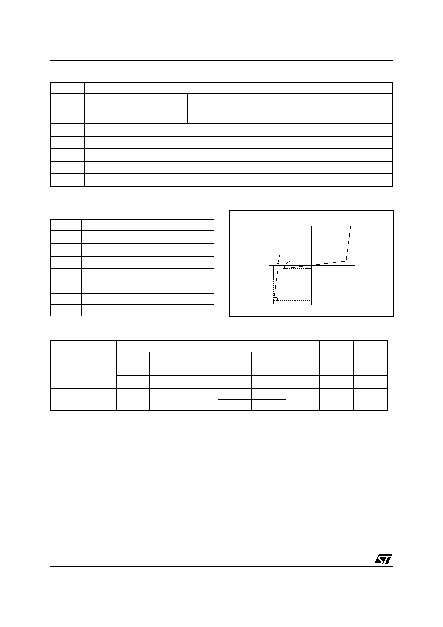
FUNCTIONAL DIAGRAM
GND
A1
A3
C1
C3
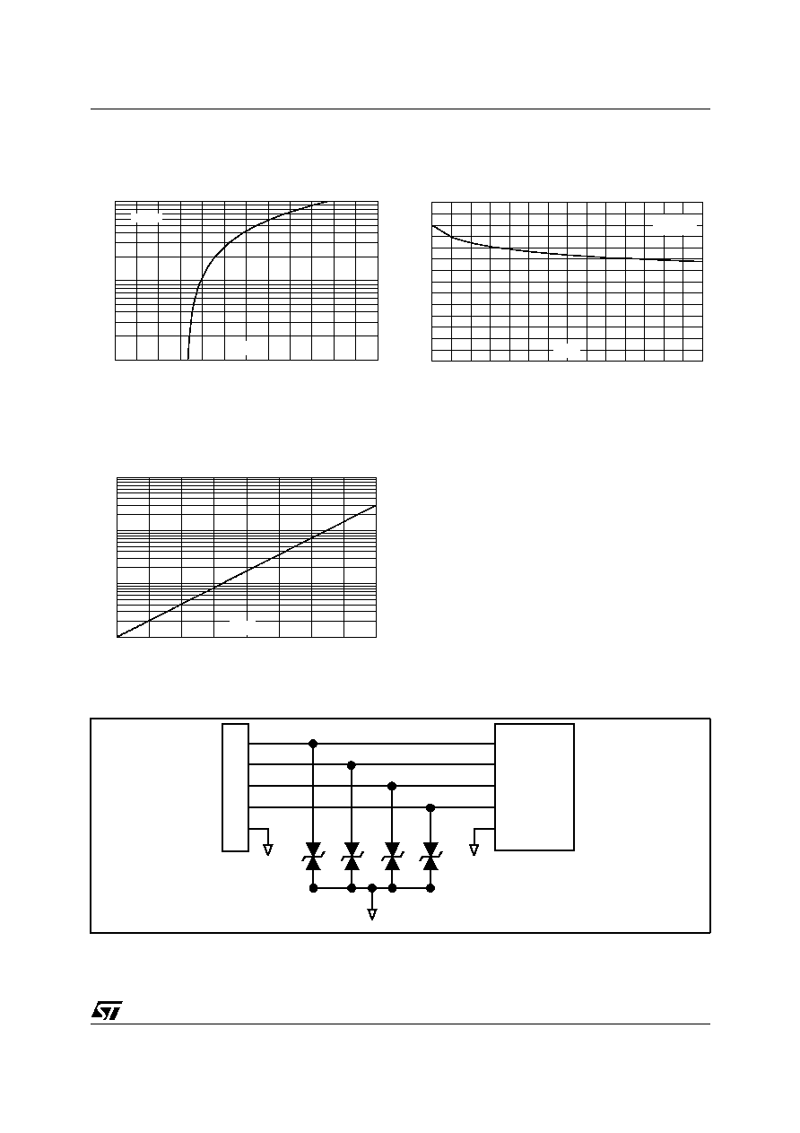
PIN CONFIGURATION (Ball Side)
A
B
C
3
1
2
ESDA14V2-4BF1
2/9
®
ABSOLUTE MAXIMUM RATING (T
amb
= 25°C)
ELECTRICAL CHARACTERISTICS (T
amb
= 25°C)
Symbol
Parameter
Value
Unit
V
PP
ESD discharge
MIL STD 883E - Method 3015-7
IEC61000-4-2 air discharge
IEC61000-4-2 contact discharge
± 25
± 15
± 8
kV
P
PP
Peak pulse power (8/20µs)
50
W
T
j
Junction temperature
125
°C
T
stg
Storage temperature range
-55 to +150
°C
T
L
Lead solder temperature (10 seconds duration)
260
°C
T
op
Operating temperature range
-40 to +125
°C
Symbol
Parameter
V
RM
Stand-off voltage
V
BR
Breakdown voltage
V
CL
Clamping voltage
I
RM
Leakage current
I
PP
Peak pulse current
C
Capacitance
Rd
Dynamic resistance
Part Number
V
BR
@ I
R
I
RM
@ V
RM
R
d
T
C
min.
max.
max.
typ.
max.
max.
note 1
note 2
0V bias
V
V
mA
µA
V
10
-4
/°C
pF
ESDA14V2-4BF1
14.2
18
1
1
12
3.2
10
15
0.1
3
Note 1: Square pulse, IPP = 3A, tp = 2.5µs.
Note 2:
VBR =
T (Tamb -25°C) x VBR (25°C)
I
V
V
BR
CL
VRM
I PP
I RM
V
Slope = 1/Rd
ESDA14V2-4BF1
3/9
®
APPLICATION EXAMPLE
Fig. 1: Clamping voltage versus peak pulse
current (Tj initial = 25°C) (Rectangular waveform).
Fig. 2: Capacitance versus reverse applied
voltage (typical values).
Fig. 3: Relative variation of leakage current versus
junction temperature (typical values).
0.1
1.0
10.0
0
10
20
30
40
50
60
V
(V)
CL
I
(A)
PP
tp = 2.5µs
0
2
4
6
8
10
12
14
0
2
4
6
8
10
12
14
V (V)
R
C(pF)
F=1MHz
V
=30mV
T =25°C
OSC
RMS
j
1
10
100
1000
25
50
75
100
125
T (°C)
j
I [T ] / I [T =25°C]
R
j
R
j
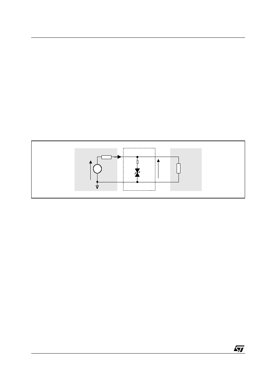
Connector
IC
to be
protected
A1
A3
C1
C3
B2
ESDA14V2-4BF1
4/9
®
TECHNICAL INFORMATION
1. ESD protection by ESDA14V2-4BF1
With the focus of lowering the operation levels, the problem of malfunction caused by the environment is
critical. Electrostatic discharge (ESD) is a major cause of failure in electronic systems.
As a transient voltage suppressor, ESDA14V2-4BF1 is an ideal choice for ESD protection by suppressing
ESD events. It is capable of clamping the incoming transient to a low enough level such that any damage
is prevented on the device protected by ESDA14V2-4BF1.
ESDA14V2-4BF1 serves as a parallel protection elements, connected between the signal line and ground.
As the transient rises above the operating voltage of the device, the ESDA14V2-4BF1 becomes a low
impedance path diverting the transient current to ground.
The clamping voltage is given by the following formula:
V
CL
= V
BR
+ R
d
.I
PP
As shown in figure A1, the ESD strikes are clamped by the transient voltage suppressor.
Fig. A1: ESD clamping behavior.
To have a good approximation of the remaining voltages at both Vi/o side, we provide the typical
dynamical resistance value R
d
. By taking into account the following hypothesis:
we have:
The results of the calculation done V
G
= 8kV, R
G
= 330
(IEC61000-4-2 standard), V
BR
= 14.2V (typ.)
and R
d
= 3.2
(typ.) give:
This confirms the very low remaining voltage across the device to be protected. It is also important to note
that in this approximation the parasitic inductance effect was not taken into account. This could be a few
tenths of volts during a few ns at the Vi/o side.
ESDA14V2-4BF1
Rg
Rd
V
BR
Vg
R load
ESD Surge
Device
to be
protected
V(i/o)
Ip
R
G
R
d
""and""R
load
R
d
>
>
V i o
/
(
) V
BR
R
d
+
V
G
R
G
--------
×
=
V i o
/
(
)
91.8 Volts
=
ESDA14V2-4BF1
5/9
®
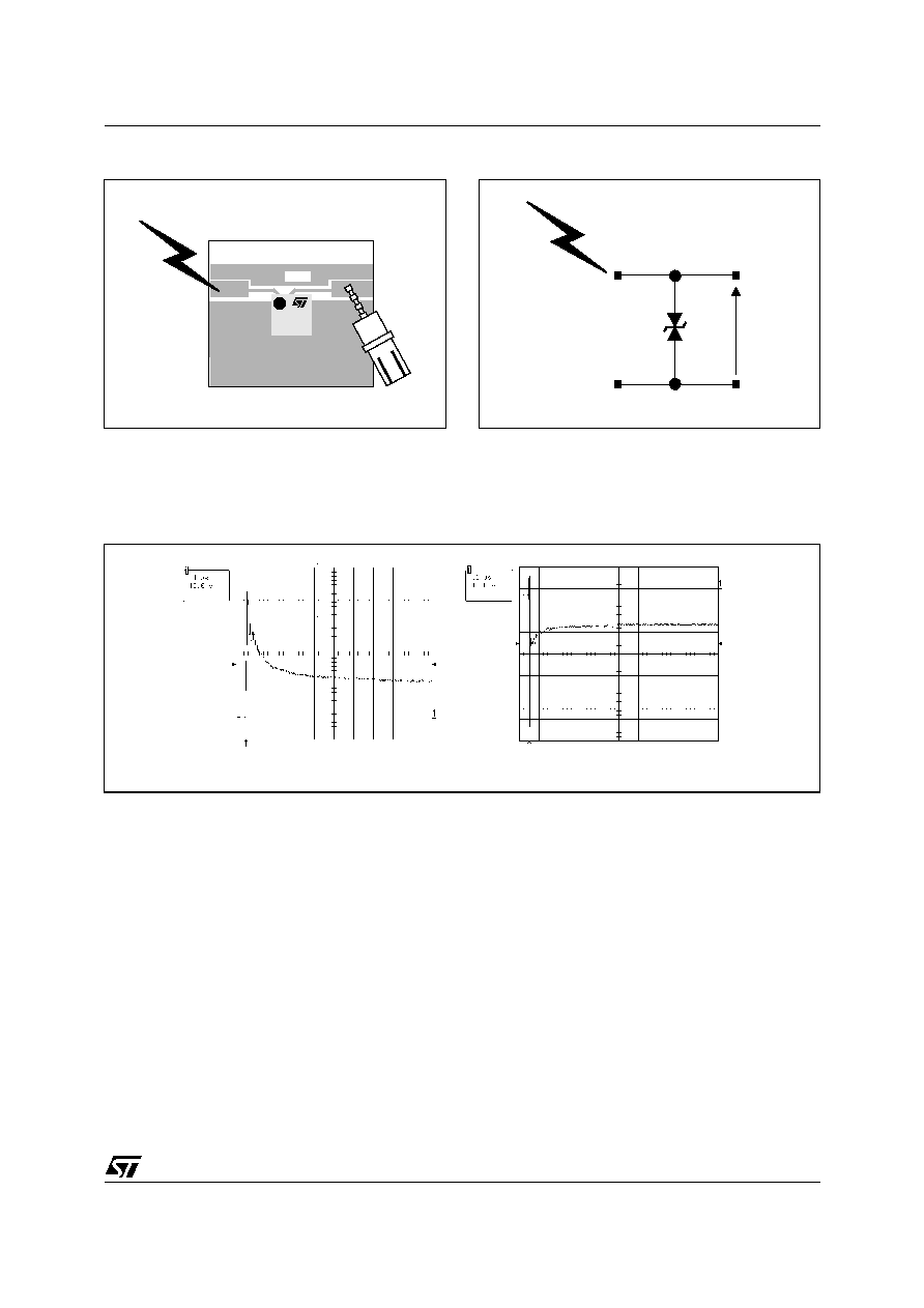
The measurements done here after show very clearly (figure A4) the high efficiency of the ESD protection:
the clamping voltage V(i/o) becomes very close to V
BR
(positive way, figure A4a) and -V
BR
(negative way,
figure A4b).
Fig. A2: ESD test board.
Fig. A3: ESD test condition.
Fig. A4: Remaining voltage during ESD surge.
TEST BOARD
V(i/o)
EB14
15
®
V(i/o)
B2
A1, C1, A3 or C3
± 15kV
ESD Air discharge
V(i/o)
V(i/o)
a: Response in the positive way
b: Response in the negative way