 | –≠–ª–µ–∫—Ç—Ä–æ–Ω–Ω—ã–π –∫–æ–º–ø–æ–Ω–µ–Ω—Ç: ESDA6V1B1 | –°–∫–∞—á–∞—Ç—å:  PDF PDF  ZIP ZIP |
ESDA6V1B1
Æ
November 1999 - Ed : 2B
6 BIDIRECTIONAL TRANSIL
TM
FUNCTIONS
LOW LEAKAGE CURRENT : I
R
MAX < 2
µ
A
200 W PEAK PULSE POWER (8/20
µ
s)
FEATURES
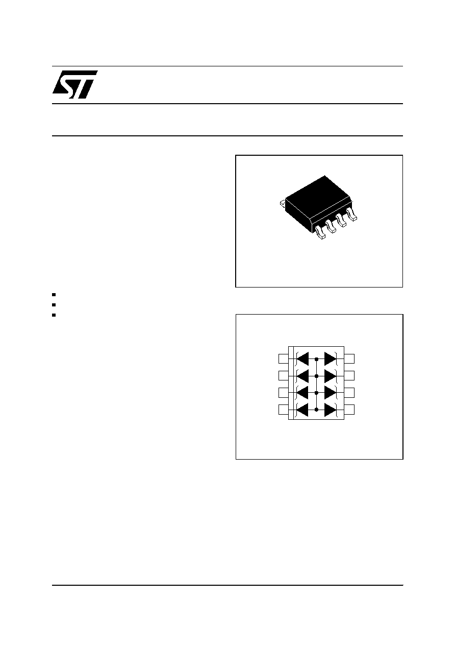
SO8
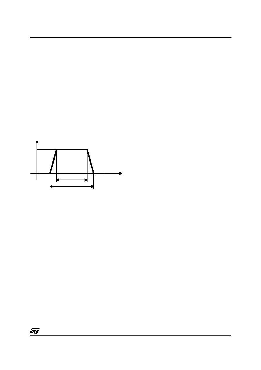
FUNCTIONAL DIAGRAM
1
2
3
4
I/O 1
I/O 2
I/O 3
GND
I/ O 6
8
7
6
5
I/ O 4
I/ O 5
GND
DESCRIPTION
The ESDA6V1B1 is a monolithic voltage
suppressor designed to protect components which
are connected to data and transmission lines
against ESD.
It clamps the voltage just above the logic level
supply for positive and negative transients.
TRANSIL
TM
ARRAY
FOR ESD PROTECTION
Application Specific Discretes
A.S.D.
TM
Where transient overvoltage protection in ESD
sensitive equipment is required, such as :
- COMPUTER
- PRINTERS
- COMMUNICATION SYSTEMS
- GSM HANDSETS AND ACCESSORIES
- CAR RADIO
It is particularly recommended for parallel port
protection where the line interface withstands only
2kV ESD surge
MAIN APPLICATIONS
BENEFITS
High ESD protection level : up to 25 kV
High integration
Suitable for high density boards
IEC 1000-4-2 : level 4
MIL STD 883C-Method 3015-6 : class 3
(human body model)
COMPLIES WITH THE FOLLOWING STANDARDS :
1/6

Symbol
Parameter
V
RM
Stand-off voltage
V
BR
Breakdown voltage
V
CL
Clamping voltage
I
RM
Leakage current
I
PP
Peak pulse current
T
Voltage temperature coefficient
C
Capacitance
Rd
Dynamic resistance
ELECTRICAL CHARACTERISTICS (T
amb
= 25∞C)
Symbol
Parameter
Value
Unit
V
PP
Electrostatic discharge
MIL STD 883C - Method 3015-6
25
kV
P
PP
Peak pulse power (8/20
µ
s)
200
W
T
stg
T
j
Storage temperature range
Maximum junction temperature
- 55 to + 150
150
∞
C
∞
C
T
L
Maximum lead temperature for soldering during 10s
260
∞
C
ABSOLUTE MAXIMUM RATINGS (T
amb
= 25∞C)
Types
V
BR
@
I
R
I
RM
@ V
RM
Rd
T
C
min.
max.
max.
typ.
max.
typ.
note 1
note 2
note 3
0V bias
V
V
mA
µ
A
V
10
-4
/
∞
C
pF
ESDA6V1B1
6.1
8
1
2
5
0.7
10
50
note 1 : Between two I/O pins or I/O pin and Groung
note 2 : Square pulse, Ipp = 25A, tp=2.5
µ
s.
note 3 :
VBR =
T* (Tamb -25∞C) * VBR (25∞C)
ESDA6V1B1
2/6
The ESDA family has been designed to clamp fast
spikes like ESD. Generally the PCB designers
need to calculate easily the clamping voltage V
CL
.
This is why we give the dynamic resistance in
addition to the classical parameters. The voltage
across the protection cell can be calculated with
the following formula:
V
CL
= V
BR
+ Rd I
PP
Where Ipp is the peak current through the ESDA cell.
DYNAMIC RESISTANCE MEASUREMENT
The short duration of the ESD has led us to prefer
a more adapted test wave, as below defined, to the
classical 8/20
µ
s and 10/1000
µ
s surges.
2.5
µ
s duration measurement wave.
As the value of the dynamic resistance remains
stable for a surge duration lower than 20
µ
s, the
2.5
µ
s rectangular surge is well adapted. In addition
both rise and fall times are optimized to avoid any
parasitic phenomenon during the measurement of
Rd.
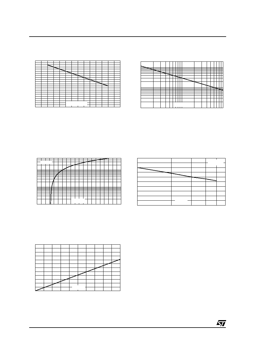
CALCULATION OF THE CLAMPING VOLTAGE
USE OF THE DYNAMIC RESISTANCE
2µs
tp = 2.5µs
t
I
Ipp
ESDA6V1B1
3/6
0
25
50
75
100
125
150
175
0.0
0.1
0.2
0.3
0.4
0.5
0.6
0.7
0.8
0.9
1.0
1.1
Ppp[Tj initial]/Ppp[Tj initial=25∞C]
Tj initial(∞C)
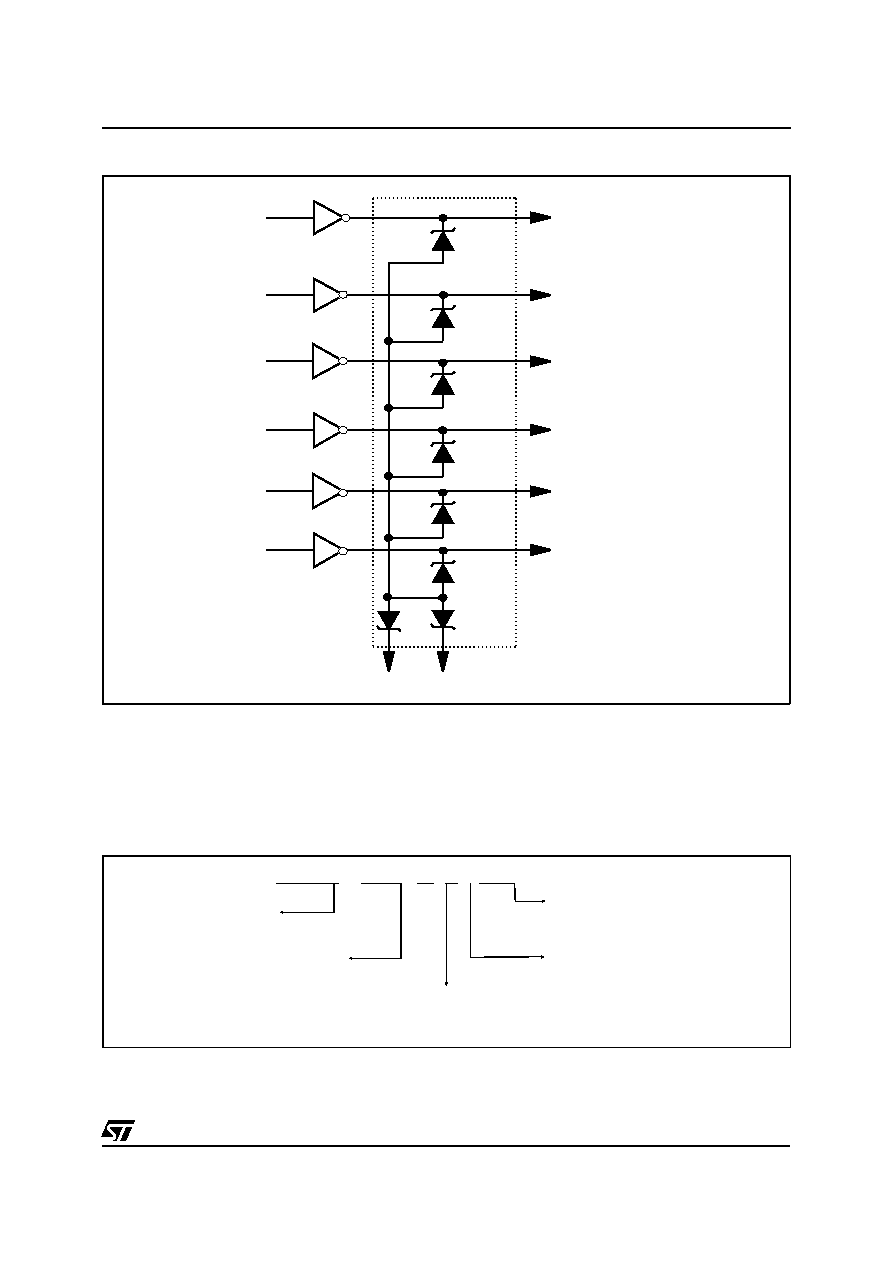
Fig. 1 : Peak power dissipation versus initial
junction temperature.
0
5
10
15
20
25
30
35
40
45
50
0.1
1.0
10.0
50.0
Ipp(A)
tp=2.5µs
Vcl(V)
Fig. 3 : Clamping voltage versus peak pulse
current (Tj initial = 25 ∞C).
Rectangular waveform tp = 2.5
µ
s.
1
10
100
10
100
1000
2000
Ppp(W)
tp(µs)
Fig. 2 : Peak pulse power versus exponential
pulse duration (Tj initial = 25 ∞C).
1
2
3
4
6
5
25
30
35
40
45
50
C(pF)
F=1MHz
Vosc=30mV
VR(V)
Fig. 4 : Capacitance versus reverse applied
voltage (typical values).
25
50
75
100
125
150
1.0
1.2
1.4
1.6
1.8
2.0
2.2
IR[Tj] / IR[Tj=25∞C]
Tj(∞C)
Fig. 5 : Relative variation of leakage current versus
junction temperature (typical values).
ESDA6V1B1
4/6
APPLICATION EXAMPLE: Protection of symmetrical signals.
+/- 2.5 V
A6
6.1V
A1
6.1V
+/- 2.5 V
A2
+/- 2.5 V
6.1V
A3
+/- 2.5 V
6.1V
6.1V
+/- 2.5 V
A4
6.1V
A5
6.1V
+/ 2.5 V
-
ORDER CODE
ESDA 6V1 B 1
RL
ESD ARRAY
V
BR
min
PACKAGE : SO8
Bidirectional
PACKAGING:
RL = Tape and reel
= Tube
ESDA6V1B1
5/6
MARKING : Logo, Date Code, E6V1B1
Packaging : Preferred packaging is tape and reel.
Weight : 0.08g.
Information furnished is believed to be accurate and reliable. However, STMicroelectronics assumes no responsibility for the consequences of
use of such information nor for any infringement of patents or other rights of third parties which may result from its use. No license is granted by
implication or otherwise under any patent or patent rights of STMicroelectronics. Specifications mentioned in this publication are subject to
change without notice. This publication supersedes and replaces all information previously supplied.
STMicroelectronics products are not authorized for use as critical components in life support devices or systems without express written ap-
proval of STMicroelectronics.
The ST logo is a registered trademark of STMicroelectronics
© 1999 STMicroelectronics - Printed in Italy - All rights reserved.
STMicroelectronics GROUP OF COMPANIES
Australia - Brazil - China - Finland - France - Germany - Hong Kong - India - Italy - Japan - Malaysia
Malta - Morocco - Singapore - Spain - Sweden - Switzerland - United Kingdom - U.S.A.
http://www.st.com
L
E
D
8
4
5
1
M
S
c1
e
b
e3
A
C
a1
b
a3
1
a2
F
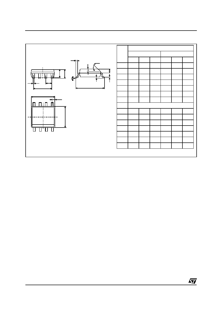
PACKAGE MECHANICAL DATA
SO8 Plastic
REF.
DIMENSIONS
Millimetres
Inches
Min. Typ. Max. Min. Typ. Max.
A
1.75
0.069
a1
0.1
0.25 0.004
0.010
a2
1.65
0.065
a3
0.65
0.85 0.025
0.033
b
0.35
0.48 0.014
0.019
b1
0.19
0.25 0.007
0.010
C
0.25
0.50
0.50 0.010
0.020
c1
45∞ (typ)
D
4.8
5.0
0.189
0.197
E
5.8
6.2
0.228
0.244
e
1.27
0.050
e3
3.81
0.150
F
3.8
4.0
0.15
0.157
L
0.4
1.27 0.016
0.050
M
0.6
0.024
ESDA6V1B1
6/6