August 2006
Rev 1
1/7
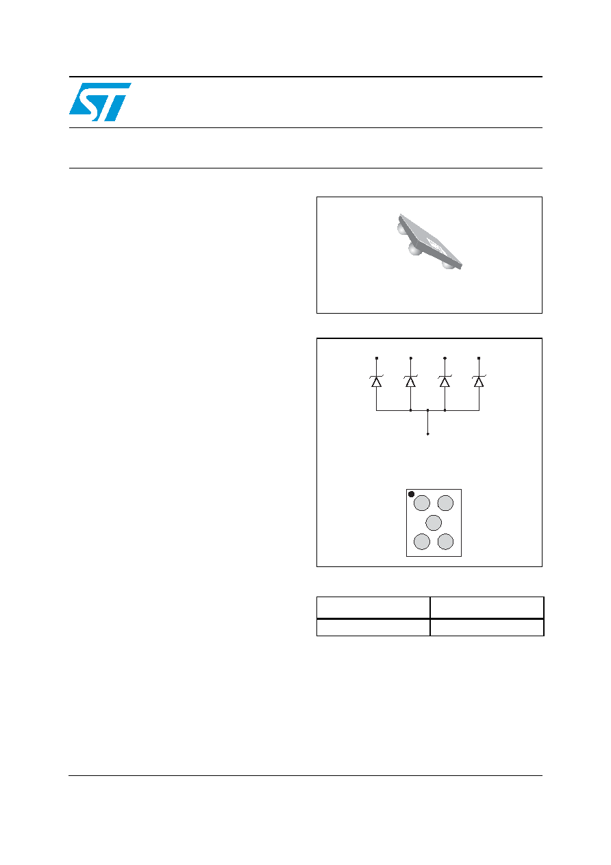
ESDALC6V1F2
Quad low capacitance TRANSILTM array for ESD protection
Applications
Where transient overvoltage protection in ESD
sensitive equipment is required, such as:
Computers
Printers
Communication systems and cellular phones
Video equipment
This device is particularly adapted to the
protection of symmetrical signals
Features
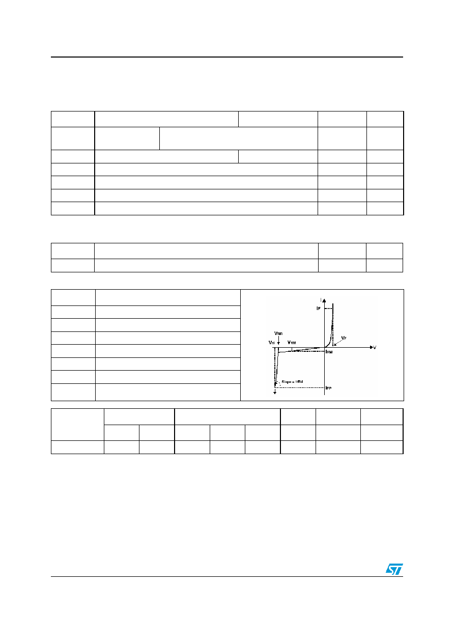
4 unidirectional TRANSIL functions.
Breakdown voltage V
BR
= 6.1 V min.
Low diode capacitance (12 pF @ 0 V)
Low leakage current (< 500 nA @ 3 V)
very small PCB area (1.33 mm
2
)
Lead free package
Benefits
High ESD protection level
High integration
Suitable for high density boards
Description
The ESDALC6V1F2 is a monolithic array
designed to protect up to 4 lines againast ESD
transients. The device is ideal for applications
where both reduced line capacitance and board
space saving are required.
TM: TRANSIL is a trademark of STMicroelectronics
Functional diagram
Order code
Complies with the following standards:
Part number
Marking
ESDALC6V1F2
EDT
IEC61000-4-2
15 kV (air discharge)
8 kV (contact discharge)
MIL STD 883E - Method 3015-7: class 3
25 kV (Human body model)
Lead free Flip-Chip
(5 bumps)
B2
A1
A3
C1
C3
A B C
1
2
3
www.st.com
Characteristics
ESDALC6V1F2
2/7
1 Characteristics
Table 1.
Absolute maximum ratings (T
amb
)= 25 °C
Symbol
Parameter
Value
Unit
V
PP
ESD discharge
IEC61000-4-2 air discharge
IEC61000-4-2 contact discharge
± 15
± 8
kV
P
PP
Peak pulse power dissipation (8/20 µs.
(1)
T
j initial
= T
amb
25
W
T
j
Junction temperature
125
°C
T
stg
Storage temperature
- 55 to +150
°C
T
L
Maximum lead temperature for soldering during 10 s at 5 mm for case
260
°C
T
OP
Operating temperature range
- 40 to + 125
°C
1.
For a surge greater than the maximum values, the diode will fail in short-circuit
Table 2.
Thermal resistance
Synbol
Parameter
Value
Unit
R
th(j-a)
Junction to ambient on printed circuit on recommended pad layout
150
°C/W
Table 3.
Electrical characteristics
Symbol
Parameter
V
RM
Stand-of voltage
V
BR
Breakdown voltage
V
CL
Clamping voltage
I
RM
Leakage current @ V
RM
I
PP
Peak pulse current
T
Voltage temperature coefficient
V
F
Forward voltage drop
Type
I
RM
@ V
RM
V
BR
@ I
R
R
D
T
C
µA max
V
Vmin
Vmax
mA
Typ
10-4/°C max pFtyp @0 V
ESDALC6V1F2
0.5
3
6.1
7.2
1
1
5
12
ESDALC6V1F2
Characteristics
3/7
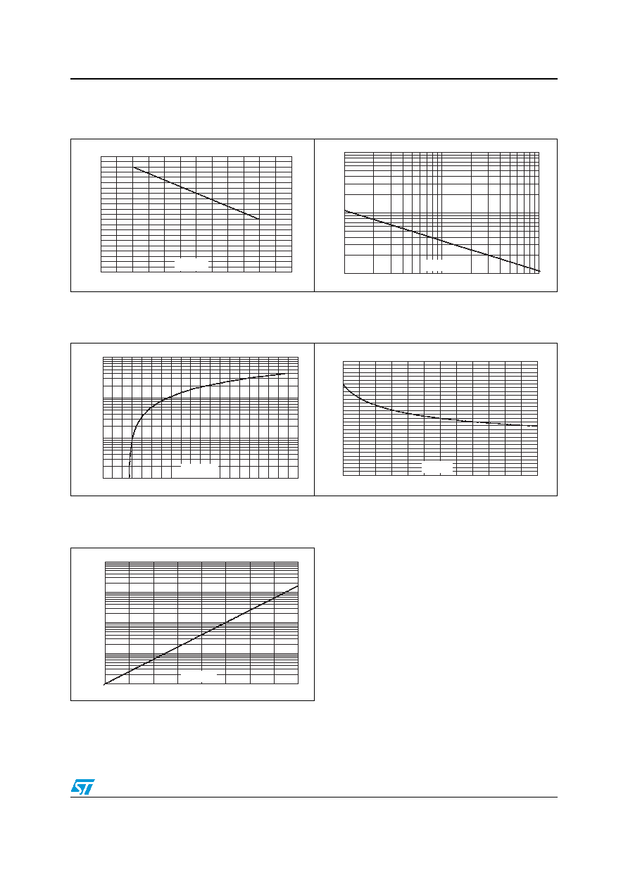
Figure 1.
Peak power dissipation versus
initial junction temperature
Figure 2.
Peak pulse power versus
exponential pulse duration
(T
j
initial = 25°C)
0.0
0.1
0.2
0.3
0.4
0.5
0.6
0.7
0.8
0.9
1.0
1.1
0
25
50
75
100
125
150
P
PP
[T
j
initial] / P
PP
[T
j
initial=25°C]
T
j
(°C)
10
100
1000
1
10
100
P
PP
(W)
t
P
(µs)
Figure 3.
Clamping voltage versus peak
pulse current (T
j
initial = 25°C),
rectangular waveform t
p
= 2.5 µs).
Figure 4.
Capacitance versus reverse applied
voltage (typical values)
Figure 5.
Relative variation of the leakage
current versus junction
temperature (typical values)
0.1
1.0
10.0
100.0
0
5
10
15
20
25
30
35
40
45
50
I
PP
(A)
V
CL
(V)
0
1
2
3
4
5
6
7
8
9
10
11
12
13
14
15
0
1
2
3
4
5
6
C(pF)
V
R
(V)
1.E+00
1.E+01
1.E+02
1.E+03
1.E+04
25
50
75
100
125
I
R
[T
j
] / I
R
[T
j
=25°C]
T
j
(°C)
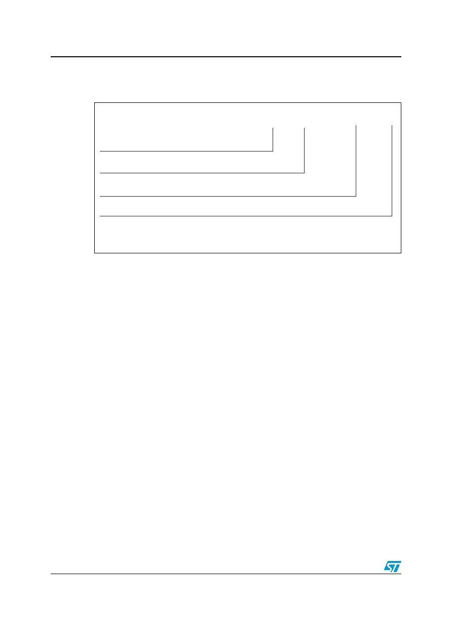
Ordering information scheme
ESDALC6V1F2
4/7
2
Ordering information scheme
ESDA LC - 6V1 F2
ESD Array
Low capacitance
VBR min = 6.1 V
Package
F = Flip-Chip
2 = Leadfree Pitch = 500µm, Bump = 315µm
ESDALC6V1F2
Package information
5/7
3 Package
information
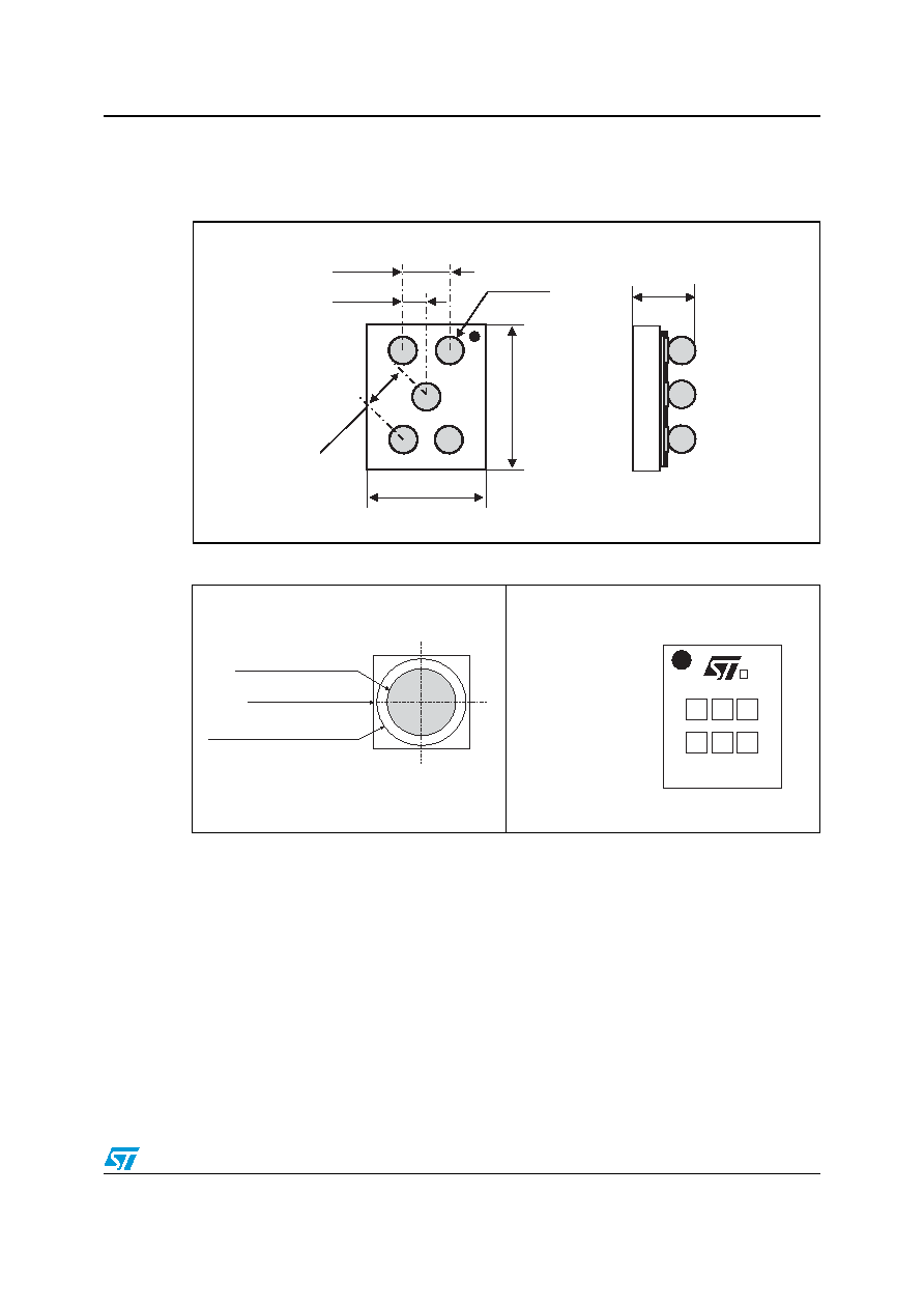
Figure 6.
Flip-Chip dimensions
Figure 7.
Flip-Chip footprint
Figure 8.
Marking
0.95 mm ± 50µm
1.32 mm ± 50µm
500µm ± 15
315µm ± 50
500µm ± 10
250µm ± 10
650µm ± 50
Copper pad Diameter :
250µm recommended , 300µm max
Solder stencil opening : 330µm
Solder mask opening recommendation :
340µm min for 315µm copper pad diameter
Dot, ST logo
xx = marking
yww = datecode
(y = year ww = week)
z = manufacturing location
x
y
x
w
z
w
E